|
|||||||||||||
 |
|||||||||||||
The 1-dB Compression Point - Its History, Meaning, and Calculation© |
|||||||||||||
|
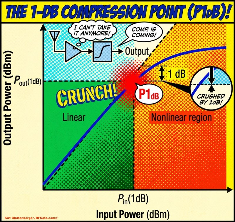
1. Executive Summary The 1-dB compression point, usually written P1dB, is a practical large-signal linearity limit for RF and microwave components such as low-noise amplifiers, power amplifiers, mixers, active frequency multipliers, driver stages, variable-gain amplifiers, attenuators, limiters, isolators, filters, switches, and receiver front-end modules. It is the input or output power level at which the measured gain has fallen 1 dB below the gain predicted by the small-signal linear gain line. In symbols, if the small-signal gain is GSS in dB, then at the 1-dB compression point: Pout(measured, dBm) = Pin(dBm) + GSS(dB) - 1 dB When the input power at that condition is quoted, it is called input P1dB, IP1dB, or P1dB,in. When the output power is quoted, it is called output P1dB, OP1dB, or P1dB,out. Unless a data sheet says otherwise, RF power-amplifier data sheets often emphasize OP1dB, while receiver front-end and mixer data sheets often list both input-referred and output-referred values. P1dB occurs because real electronic devices are not perfectly linear. Transistors run out of voltage swing, current swing, transconductance, bias headroom, or load-line margin. Diodes in mixers and limiters become strongly nonlinear. Ferrites, magnetic materials, dielectric materials, and resistive films can heat or saturate. At small signal levels, the output of a device is nearly proportional to the input. At higher levels, the incremental gain falls. The output power still may increase, but it increases more slowly than the ideal straight-line prediction. Electronics & Technology
P1dB is important because it marks the approximate boundary between comfortably linear operation and visibly compressed operation. Compression changes both amplitude and phase behavior, produces harmonic distortion, increases intermodulation distortion, causes spectral regrowth for digitally modulated signals, worsens error-vector magnitude, degrades adjacent-channel leakage ratio, and can desensitize receivers. In transmitters, operating near or beyond P1dB can violate spectral masks and create interference. In receivers, a strong blocker can compress the LNA, mixer, IF amplifier, or ADC driver, reducing desired-signal gain and raising distortion products. Excessive drive can also produce damaging power dissipation, especially in power amplifiers, mixer diodes, ferrite isolator loads, attenuators, filters, switches, and other parts with finite average-power, peak-power, voltage, current, or thermal ratings. The standard measurement method is straightforward: apply a single CW tone from a calibrated signal generator, increase input power in steps, measure fundamental output power with a power meter, spectrum analyzer, or vector/signal analyzer, and compare the measured output to the extrapolated small-signal gain line. The input and output power at which the measured output is 1 dB below the extrapolated line are the input and output P1dB values. Accurate measurement requires correction for cable loss, attenuator loss, mismatch, sensor calibration, analyzer compression, harmonic content, bandwidth, device heating, duty cycle, and bias conditions. Cascade Calculation Approximation For cascaded RF chains, there is no exact universal closed-form P1dB cascade equation because P1dB is a large-signal gain-compression condition and depends on the detailed nonlinear transfer curves of all stages. A common engineering approximation is to use an equation shaped like the cascaded third-order intercept point, IP3, equation. In linear power units: 1 / P1dB,in,total approximately equals 1 / P1dB,in,1 + G1 / P1dB,in,2 + G1G2 / P1dB,in,3 + … where all powers are in watts or milliwatts, and gains G are linear power gains, not dB. This method is often useful for quick receiver and transmitter budget estimates, but it is only an approximation. It assumes that compression contributions can be combined in a reciprocal-power form similar to small-signal third-order distortion contributions. Real compression is affected by higher-order nonlinearities, device memory effects, AM-to-PM conversion, impedance mismatch, harmonic terminations, mixer LO drive, temperature, bias shift, and the shapes of the individual gain-compression curves. Errors of several dB are possible, and larger errors can occur when multiple stages compress at about the same chain input level, when one stage has hard limiting, or when stage nonlinearities partially cancel or reinforce. The analysis of nonlinear RF behavior did not come from a single inventor. It grew out of mathematical nonlinear-system theory and practical telephone, radio, and microwave engineering. Important historical foundations include Vito Volterra's functional-series treatment of nonlinear systems in Italy; Norbert Wiener's work at MIT on nonlinear and random-system theory; Bell Telephone Laboratories work by engineers such as Harold S. Black, Hendrik W. Bode, William R. Bennett, and Harald T. Friis; and later RF/microwave system-design texts and application notes by authors and organizations such as Stephen A. Maas, William F. Egan, David M. Pozar, Steve C. Cripps, Keysight, Rohde & Schwarz, Analog Devices, Mini-Circuits, Marki Microwave, Qorvo, and others. The modern P1dB measurement procedure is best understood as an industry-standard measurement convention rather than as a named theorem attributable to one person. 2. Key Findings • P1dB is the power level where actual gain is 1 dB less than the extrapolated small-signal gain. • P1dB may be specified as input-referred IP1dB or output-referred OP1dB. For a single device in the small-signal region, OP1dB is approximately IP1dB + small-signal gain in dB - 1 dB when OP1dB means the measured compressed output power. Some data sheets, however, use slightly different conventions, so the definition should be checked. • The physical cause is nonlinear device behavior: transistor transconductance curvature, current limiting, voltage swing limiting, saturation, cutoff, knee-voltage effects, bias shift, self-heating, magnetic saturation, diode conduction changes, and other large-signal mechanisms. • In a transmitter, compression creates harmonic distortion, intermodulation distortion, spectral regrowth, degraded EVM, degraded ACLR/ACPR, and possible violation of regulatory emission masks. • In a receiver, compression from strong blockers reduces gain for the desired signal, creates intermodulation products, can overload mixers or IF stages, and may drive ADCs or detector stages into clipping. • P1dB is not the same as maximum safe input power, absolute maximum rating, saturated output power, Psat, damage threshold, or safe operating area. A device may be damaged below, near, or above P1dB depending on thermal design, duty cycle, mismatch, bias, and power rating. • The standard P1dB test is a single-tone swept-power measurement. A calibrated generator drives the device under test, and the fundamental output power is measured while input power is stepped upward. • A broadband power meter can overstate fundamental output power if harmonics are significant. For a strict fundamental-power P1dB measurement, use a spectrum analyzer, signal analyzer, tuned receiver, or harmonic filter before the power meter. • Cascaded P1dB estimates are usually made by converting every stage's P1dB and gain to linear units, referring all stage compression levels to the cascade input or output, and combining them with a reciprocal-power formula similar to the cascaded IP3 formula. • The P1dB cascade formula is approximate because P1dB is a large-signal compression condition, while IP3 is based on small-signal extrapolation of third-order intermodulation products. • For a simple memoryless cubic nonlinearity, the two-tone third-order intercept point is often about 9.6 dB above P1dB. Many RF devices show a rough OIP3-to-OP1dB spacing of about 6 dB to 12 dB, but the value is technology-, frequency-, bias-, and load-dependent. • For modern digitally modulated transmitters, P1dB is often less predictive of real system performance than ACLR, ACPR, EVM, noise-power ratio, crest-factor behavior, and digital predistortion performance. 3. Detailed Analysis 3.1 Definition of 1-dB Compression Point An ideal linear RF device has a constant gain. If input power increases by 1 dB, output power also increases by 1 dB. On a graph of Pout in dBm versus Pin in dBm, the linear region is a straight line with slope 1. The small-signal gain is the vertical separation between output and input power in this low-level region. At higher drive levels, real devices depart from that ideal line. The most common departure is gain compression, where the output still rises as input increases, but not as fast as expected. The 1-dB compression point is the point where the measured output is 1 dB below the output predicted by extending the small-signal gain line. Small-signal predicted output: Poutideal(dBm) = Pin(dBm) + GSS(dB) 1-dB compression condition: Poutmeasured(dBm) = Poutideal(dBm) - 1 dB or: Gainmeasured(dB) = GSS(dB) - 1 dB If the input power at this point is quoted, it is IP1dB. If the output power at this point is quoted, it is OP1dB. For example, suppose an amplifier has 20 dB small-signal gain. At Pin = 0 dBm, the linear prediction is Pout = +20 dBm. If the measured output is +19 dBm, the amplifier is at its 1-dB compressed output condition. In this example, IP1dB is 0 dBm and OP1dB is +19 dBm, assuming OP1dB is defined as measured output power at compression. Some manufacturers define output P1dB as the extrapolated output power rather than the measured output power. The difference is exactly 1 dB. Most RF data sheets use the measured compressed output power, but the convention is not universal. This is one reason careful engineers read the test conditions and definitions in the data sheet. Industry sources such as Mini-Circuits and Keysight describe P1dB in essentially this way: it is the point where the gain has compressed by 1 dB relative to the small-signal gain line. See Mini-Circuits, "Understanding P1dB," and Keysight RF/microwave measurement application literature, for example. 3.2 Why 1 dB? The choice of 1 dB is a convention. It is large enough to be measurable with ordinary RF test equipment and small enough to represent the onset of significant nonlinearity before deep saturation. Other compression points are also used, such as 0.1-dB compression for precision instrumentation, 0.5-dB compression for some receiver calculations, 2-dB or 3-dB compression for saturated power-amplifier behavior, and Psat for near-saturation operation. But P1dB is the most common single-number large-signal linearity specification. A 1-dB gain reduction means the power gain has fallen to: 10^(-1/10) = 0.794 of the small-signal power gain. In voltage terms, for the same impedance, the voltage gain ratio is: 10^(-1/20) = 0.891 Thus, at P1dB the output voltage amplitude is about 89.1 percent of what a perfectly linear extrapolation would predict, and the output power at the fundamental is about 79.4 percent of the ideal extrapolated fundamental power. 3.3 Physical Causes of Compression Compression is not one single physical effect. It is the measured result of many possible nonlinear mechanisms. Transistor Transconductance Curvature. Voltage and Current Swing Limits. Bias Shift and Rectification. Self-Heating. Nonlinear Capacitance and Charge Storage. Mixer Diode or Switching-Device Limits. Magnetic and Ferrite Effects. Passive Component Heating. 3.4 Mathematical View of Compression A memoryless nonlinear device can be approximated over a limited range by a power series: vout = a1 vin + a2 vin^2 + a3 vin^3 + a4 vin^4 + … For many RF amplifiers operating in a reasonably symmetric region, the odd-order terms are especially important for in-band distortion. If the input is a single sinusoid: vin = A cos(wt) the cubic term contributes both a fundamental-frequency term and a third-harmonic term: cos^3(wt) = 3/4 cos(wt) + 1/4 cos(3wt) Therefore the fundamental component is approximately: vout,fundamental = [a1 A + 3/4 a3 A^3 + …] cos(wt) If a3 has a sign that opposes a1, the cubic contribution reduces the fundamental gain as A increases. That is gain compression. If a3 reinforces a1 at first, a device can show gain expansion before eventually compressing due to higher-order terms or hard limits. For a two-tone input, cubic terms generate third-order intermodulation products at frequencies 2f1 - f2 and 2f2 - f1. This is the basis for the third-order intercept point, IP3. Analog Devices gives a clear tutorial discussion of intermodulation and intercept points in MT-012, "Intermodulation Distortion Considerations for ADCs." 3.5 Relationship Between P1dB and IP3 P1dB and IP3 are both linearity measures, but they are not the same thing. P1dB is a measured large-signal single-tone gain-compression point. IP3 is an extrapolated small-signal two-tone intermodulation figure. IP3 is not normally reached physically; it is the hypothetical point where extrapolated fundamental output and extrapolated third-order intermodulation output would be equal. For an ideal memoryless cubic nonlinearity, the input-referred third-order intercept point is about 9.6 dB above the input-referred 1-dB compression point. The same approximate difference applies to output-referred values if gain is handled consistently. The derivation assumes only a first-order and third-order term, no higher-order terms, no memory, and a simple compressive cubic coefficient. Real RF devices often depart from this simple model. As a rough rule of thumb, OIP3 may be about 6 dB to 12 dB above OP1dB, but exceptions are common. Some devices with feedback, predistortion, gain expansion, hard limiting, or unusual biasing can differ significantly. For formal derivations one should consult nonlinear microwave texts such as Stephen A. Maas, "Nonlinear Microwave and RF Circuits." 3.6 Spectral Effects of Compression Compression affects spectral content in several ways. Harmonic Distortion. Intermodulation Distortion. IM3 products: 2f1 - f2 and 2f2 - f1 Fifth-order products can also fall near the desired band: IM5 products include 3f1 - 2f2 and 3f2 - 2f1 As compression deepens, higher-order products become more important, and simple IP3-based predictions become less accurate. Spectral Degrowth. Error-Vector Magnitude Degradation. Noise-Like Distortion. Receiver Desensitization. 3.7 Damage and Excess Power Dissipation P1dB is a linearity specification, not a damage specification. However, operation near or beyond P1dB often increases stress and can lead to damage if ratings are exceeded. For an RF power amplifier, a simplified power balance is: Pdissipated approximately equals PDC + PRF,in - PRF,out - other extracted RF power In practice, harmonic power, reflected power, load mismatch, bias network loss, package loss, and thermal impedance must also be considered. If the amplifier is driven harder after compression, additional input and DC power may mostly become heat rather than useful fundamental RF output. Junction temperature rises. Excess temperature can cause parameter drift, metallization failure, electromigration, bond-wire failure, solder fatigue, package delamination, or catastrophic transistor failure. In bipolar devices, high voltage and current can cause second breakdown or avalanche-related damage. In MOSFET, LDMOS, and GaN devices, excessive voltage swing, gate overdrive, drain voltage, current density, or channel temperature can damage the device. GaN devices can tolerate high power density, but they still require careful thermal design and operation within rated voltage, current, RF drive, and load mismatch limits. In mixers, excessive RF, LO, or IF power can damage Schottky diodes, FET gates, transformer windings, baluns, or terminations. Passive mixers often have relatively high linearity, but their maximum RF and LO power ratings must be respected. In isolators and circulators, the forward path may handle high power, but the internal load is rated for only a certain amount of reflected power. If a power amplifier is compressed or saturated into a bad VSWR, the isolator load can overheat while absorbing reflected power. In filters, duplexers, switches, and attenuators, high power can cause dielectric heating, arcing, varactor or PIN-diode damage, resistor-film failure, connector heating, and changes in insertion loss. A component may remain linear up to a high power level but still be thermally damaged by average power or peak voltage. Therefore, system designers should check at least four different kinds of limits: • Linear operating limit, such as P1dB, IP3, EVM, or ACLR requirement. 3.8 Standard Single-Tone P1dB Measurement Method The standard bench measurement uses a signal generator, the device under test, calibrated attenuation or coupling, and a power-measuring instrument. Typical Equipment: Measurement Procedure: 1. Set the device to its specified operating conditions: supply voltage, bias current, LO drive for mixers, temperature, frequency, termination impedances, and modulation state if applicable. 2. Calibrate or account for input cable loss, output cable loss, attenuator loss, coupler coupling factor, power sensor calibration factor, and analyzer amplitude accuracy. 3. Apply a low-level CW input tone well below compression. Measure output power. Calculate small-signal gain: GSS(dB) = Pout(dBm) - Pin(dBm) 4. Increase input power in small steps, commonly 0.25 dB, 0.5 dB, or 1 dB steps. At each step, measure fundamental output power. 5. Compute the compressed gain at each point: G(Pin) = Pout(Pin) - Pin 6. Find the point where: G(Pin) = GSS - 1 dB 7. Interpolate between measurement points if necessary. The corresponding input power is IP1dB. The measured output power is OP1dB. 8. Verify that the measurement instrument is not itself compressed. A spectrum analyzer front end, mixer, preamplifier, or power sensor can compress if overdriven. Use sufficient external attenuation and check analyzer linearity. 9. For high-power or thermally sensitive devices, use pulsed measurements or controlled dwell time if the data sheet specifies pulsed P1dB. Continuous-wave P1dB and pulsed P1dB can differ because of heating. Power Meter Versus Spectrum Analyzer: A power meter is accurate for total RF power over its sensor bandwidth, but it may measure harmonics along with the fundamental. If compression produces significant harmonic power, the power meter reading may be higher than the fundamental output power. A spectrum analyzer or signal analyzer can measure the fundamental alone, but it must be calibrated and operated below its own compression level. A narrowband receiver or a power meter preceded by a low-pass, band-pass, or tunable filter can also be used. Using a Vector Network Analyzer: Many VNAs can perform power sweeps and measure gain compression directly. The VNA source is swept in power, and S21 is measured as a function of input level. For high-power devices, external amplifiers, couplers, attenuators, and receivers may be required. Large-signal network analyzers and nonlinear VNAs can measure waveform, phase, harmonic, and load-pull behavior. Joel Dunsmore's "Handbook of Microwave Component Measurements" is a useful reference for modern VNA-based measurements. 3.9 Important Measurement Cautions Mismatch and Transducer Gain. Thermal Settling. Frequency Dependence. Bias Dependence. Harmonic Terminations. Analyzer Compression. Fundamental Versus Total Output Power. 3.10 P1dB in Transmit Chains In a transmitter, the RF chain may include a modulator, upconverter, variable-gain amplifier, driver amplifier, filter, power amplifier, isolator, coupler, duplexer, and antenna switch. Each active stage has a finite P1dB. Some passive stages also have power-handling or compression-like limits. The final power amplifier usually dominates transmitter compression because it operates at the highest power. However, earlier driver stages can also compress, especially if too much gain is placed before them. Compression in a driver stage can be particularly undesirable because the final PA may amplify the driver's distortion products. For constant-envelope modulation such as ideal FM, FSK, or some phase-modulated waveforms, a saturated or compressed amplifier may be acceptable if phase distortion and occupied bandwidth remain within limits. For amplitude-varying modulation such as AM, SSB, QAM, OFDM, LTE, 5G NR, and Wi-Fi, compression directly distorts the envelope and causes spectral regrowth. These systems often operate with output back-off from P1dB or Psat. The required back-off depends on waveform crest factor, linearity requirement, digital predistortion, feedback, and regulatory mask. For a digitally modulated transmitter, P1dB alone is rarely sufficient. Important measured quantities include: • Average output power. Rohde & Schwarz and Keysight publish extensive application material on modulation quality, EVM, and adjacent-channel measurements. For example, Rohde & Schwarz has general signal-analysis application notes, and Keysight has RF and microwave signal-analysis resources. 3.11 P1dB in Receive Chains In a receiver, P1dB is a large-signal handling metric. The first LNA may have excellent noise figure but limited input P1dB. A strong nearby transmitter, jammer, radar pulse, or out-of-band blocker can compress the LNA or mixer. Once a front-end stage compresses, later filtering may not remove the damage because the desired signal has already been gain-reduced or mixed with distortion products. Receiver linearity design must balance noise figure, gain distribution, filtering, P1dB, IP3, and ADC full-scale range. High gain early in the chain improves noise figure according to the Friis noise formula, but it reduces the input-referred compression level of later stages. Conversely, attenuation or filtering ahead of an LNA improves large-signal survivability and downstream linearity but worsens noise figure. The famous Friis noise formula was introduced by Harald T. Friis of Bell Telephone Laboratories in "Noise Figures of Radio Receivers," Proceedings of the IRE, 1944, DOI. Friis's paper was about noise figure, not P1dB, but the same engineering idea of referring stage quantities to a common input became fundamental in cascade analysis for noise, gain, compression, and intermodulation. Receiver P1dB is often less sensitive than IP3 for predicting weak-signal intermodulation interference, but it is important for blocker survival and desensitization. A receiver can have acceptable IP3 for moderate blockers but still fail under a very strong single blocker because of compression. 3.12 P1dB for Mixers Mixer P1dB is usually called conversion compression. For an upconverter, the output IF or RF power is compared with the small-signal conversion gain or loss. For a downconverter, the output IF power is compared with the RF input power plus conversion gain or loss. The 1-dB compression point is the RF input level, or sometimes IF output level, where conversion gain has fallen by 1 dB. Mixer P1dB depends on: • LO drive level. Passive diode-ring mixers often require a specified LO drive, such as +7 dBm, +10 dBm, +13 dBm, +17 dBm, or higher. A higher-level mixer often has better P1dB and IP3 but needs more LO power. Mini-Circuits provides many mixer application notes and data sheets that illustrate these dependencies. 3.13 P1dB for Passive Components Passive components are often assumed to have infinite P1dB for cascade calculations, but that assumption is not always valid. A passive attenuator, filter, switch, duplexer, limiter, or isolator can have finite linearity and power-handling limits. For many small-signal receiver calculations, a high-quality passive filter or attenuator has a P1dB so high that it can be ignored. For transmitters and high-power front ends, passive-component compression and damage limits must be considered carefully. For an ideal passive attenuator with loss L dB and no intrinsic nonlinearity, its "P1dB" would be infinite. In a cascade calculation it is represented simply by gain G less than 1: G = 10^(-L/10) But a real attenuator also has an average-power rating and peak-voltage rating. If its resistor film heats, the attenuation value can shift, and eventually the part can fail. Thus passive components may not compress like amplifiers, but they can still limit system power. 3.14 Cascaded P1dB: Exact Concept Consider a chain of nonlinear components connected in series. Each stage has a small-signal gain and a nonlinear gain-compression curve. If the exact output-versus-input curve of every stage is known, the most direct method is to propagate the signal through the chain numerically: Stage 1: Pout1 = f1(Pin1) The cascade P1dB is then found by comparing total output power with the extrapolated small-signal chain gain. This is the best method when measured AM-AM curves are available. It naturally handles unequal soft/hard compression, gain expansion, saturation, and multiple stages contributing simultaneously. The problem is that data sheets often provide only one number: P1dB. They do not provide the full gain-compression curve. Therefore designers use approximations. 3.15 Cascaded IP3 Equation The standard scalar cascaded input IP3 equation is: 1 / IIP3total = 1 / IIP31 + G1 / IIP32 + G1G2 / IIP33 + … + G1G2…Gn-1 / IIP3n All IIP3 values must be in linear power units, such as watts or milliwatts. All gains must be linear power gains, not dB. Losses are gains less than 1. The output-referred value is: OIP3total = IIP3total times Gtotal where: Gtotal = G1G2…Gn This equation is widely used in RF system design. It is derived by referring each stage's third-order distortion contribution to a common point and summing distortion powers or amplitudes under simplifying assumptions. More complete treatments use complex phasor addition because third-order products from different stages can have phases and may partially cancel. Practical RF system-design books such as William F. Egan, "Practical RF System Design," Wiley, and David M. Pozar, "Microwave Engineering," Wiley, cover intercept-point and cascade concepts. 3.16 Approximate Cascaded P1dB Equation A common engineering shortcut is to use the same form for input-referred P1dB: 1 / IP1dBtotal approximately equals 1 / IP1dB1 + G1 / IP1dB2 + G1G2 / IP1dB3 + … where: IP1dBn is the input 1-dB compression point of stage n in linear power units. Gn is the small-signal linear power gain of stage n. For a stage whose output P1dB is known instead of input P1dB: IP1dBn approximately equals OP1dBn / Gn when using linear units. In dB terms, approximately: IP1dBn(dBm) approximately equals OP1dBn(dBm) - Gn(dB) Some engineers include the 1-dB compressed-output convention explicitly and write: OP1dB(measured) = IP1dB + GSS - 1 dB while others use the extrapolated output convention: OP1dB(extrapolated) = IP1dB + GSS For cascade work, consistency matters. Mixing conventions can introduce a 1-dB bookkeeping error per stage or in the final reported value. After finding the input-referred cascade P1dB, the output-referred approximate value is: OP1dBtotal approximately equals IP1dBtotal times Gtotal in linear units, with the same convention caveat about measured versus extrapolated output. 3.17 Output-Referred Form of the Approximate Cascade Equation If each stage's output P1dB is known, an output-referred form can be written. Let OP1dBn be the output P1dB of stage n in linear power units. Let G1G2…Gn be the gain from the cascade input through the output of stage n. Then: 1 / IP1dBtotal approximately equals G1 / OP1dB1 + G1G2 / OP1dB2 + G1G2G3 / OP1dB3 + … Then: OP1dBtotal approximately equals Gtotal / [G1/OP1dB1 + G1G2/OP1dB2 + … + G1G2…Gn/OP1dBn] This expression again requires linear units. It is not valid if dBm and dB are inserted directly into the reciprocal equation. 3.18 Example Cascade Calculation Suppose a receiver chain has: Stage 1: LNA, gain = 15 dB, IP1dB = -10 dBm Convert gains to linear units: G1 = 10^(15/10) = 31.62 Convert IP1dB values to milliwatts: Stage 1 IP1dB = -10 dBm = 0.1 mW Use the approximate equation. The passive filter is ignored as a compression source: 1 / IP1dBtotal approximately equals 1/0.1 + (G1G2)/3.162 + (G1G2G3)/0.316 Calculate preceding gains: Before stage 3: G1G2 = 31.62 times 0.631 = 19.95 Before stage 4: G1G2G3 = 19.95 times 0.251 = 5.01 Then: 1 / IP1dBtotal approximately equals 10 + 19.95/3.162 + 5.01/0.316 1 / IP1dBtotal approximately equals 10 + 6.31 + 15.85 = 32.16 IP1dBtotal approximately equals 1 / 32.16 mW = 0.0311 mW Convert to dBm: IP1dBtotal(dBm) = 10 log10(0.0311) = -15.1 dBm Total gain: Gtotal(dB) = 15 - 2 - 6 + 20 = 27 dB Approximate output-referred cascade P1dB, using the extrapolated convention, is: OP1dBtotal approximately equals -15.1 dBm + 27 dB = +11.9 dBm If reporting measured output at 1-dB compression, one may subtract 1 dB depending on convention: OP1dBmeasured,total approximately equals +10.9 dBm This example shows an important point: the cascade input P1dB is worse than the first LNA's own -10 dBm because downstream stages are driven by the LNA gain and also contribute to total compression. Whether the exact chain really reaches 1-dB compression at -15.1 dBm depends on the actual compression curves. 3.19 Why the P1dB Cascade Equation Is Only an Approximation The IP3 cascade equation has a clearer small-signal basis than the P1dB cascade equation. IP3 is derived from low-level third-order intermodulation products that grow at a predictable 3:1 slope relative to input power, at least over a limited small-signal range. P1dB is different. It is the result of large-signal gain reduction at a specific point on a nonlinear curve. Main Reasons for Approximation Error: 1. P1dB Is Not a Small-Signal Parameter. 2. Compression Curves Have Different Shapes. 3. Compression Contributions Do Not Necessarily Add as Powers. 4. Higher-Order Nonlinearities Matter. 5. AM-to-PM Conversion Is Ignored. 6. Memory Effects Are Ignored. 7. Mixers Are Multiport Nonlinear Devices. 8. Mismatch and Standing Waves Matter. 9. Harmonic Terminations Are Not Represented. 10. Cancellation and Reinforcement Are Possible. Expected Magnitude of Errors: If one stage clearly dominates compression, the approximate cascaded P1dB is often reasonably close, perhaps within 1 dB to 2 dB. If two or more stages reach compression at similar cascade input powers, the approximation may predict a lower total P1dB because it assumes cumulative compression. Errors of several dB are common in practical chains. For hard limiters, strongly saturated PAs, mixers with unusual LO behavior, or thermally sensitive devices, the error can be larger. The only reliable answer is obtained by measuring the chain or simulating it with accurate nonlinear models. 3.20 Historical Development of Nonlinear and Cascade Analysis The concepts behind P1dB, IP3, and cascaded nonlinear analysis developed gradually from mathematics, telephone engineering, radio engineering, and microwave engineering. Vito Volterra, Italy. Norbert Wiener, MIT, Cambridge, Massachusetts. Bell Telephone Laboratories, New York and New Jersey. William R. Bennett's Bell System Technical Journal paper "New Results in the Calculation of Modulation Products," 1933, is an early and important treatment of modulation-product calculation in nonlinear systems. Harold S. Black's negative-feedback amplifier invention, developed at Bell Labs, was crucial for linear amplifier design because feedback can reduce distortion and stabilize gain. See Black, "Stabilized Feedback Amplifiers," Bell System Technical Journal, 1934. Hendrik W. Bode's work on network analysis and feedback stability became fundamental to amplifier design. See Bode's classic book "Network Analysis and Feedback Amplifier Design," Van Nostrand, 1945, widely available in library catalogs and reprints. Harald T. Friis's 1944 paper "Noise Figures of Radio Receivers" introduced the well-known noise cascade formula. Although it is not a P1dB formula, it established a central RF-system practice: refer each stage's contribution to the cascade input and combine contributions systematically. Modern RF and Microwave System-Design Literature. • Stephen A. Maas, "Nonlinear
Microwave and RF Circuits," Artech House. It is uncertain, and probably incorrect, to credit one named person with inventing the P1dB measurement or the P1dB cascade approximation. The evidence points to an engineering convention that emerged from RF amplifier testing, microwave receiver design, telephone-carrier distortion analysis, and later application-note practice. 3.21 Practical Design Rules Keep Operating Power Below P1dB When Linearity Matters. Use the Correct Metric for the Job. Place Gain Carefully in Receivers. Do Not Ignore Passive Ratings. Use Measured Curves When Possible. Beware of Modulated-Signal Peaks. Thermal Conditions Must Match the Real Application. 4. Open Questions and Debates in the Field 4.1 Is P1dB Still the Right Headline Linearity Metric? P1dB remains useful because it is simple and repeatable. However, for modern communication systems, P1dB alone often says little about actual system performance. A 5G NR or Wi-Fi transmitter may fail EVM or ACLR requirements well below P1dB. Conversely, with digital predistortion, a PA may operate near compression while still meeting spectral requirements. The industry increasingly relies on waveform-specific metrics in addition to P1dB. 4.2 How Should P1dB Be Defined for Modulated Signals? Classic P1dB is a CW single-tone measurement. Real systems use modulated signals with time-varying envelopes. A modulated waveform has average power, peak power, crest factor, bandwidth, and statistical distribution. There is no single universally accepted "modulated P1dB" definition. Some engineers use gain compression versus average power; others evaluate compression on peaks; others use EVM or ACLR thresholds instead. 4.3 How Accurate Is the IP3-Like P1dB Cascade Approximation? The approximation is convenient and widely used, but it is not rigorous. The debate is not whether it is exact; it is not. The practical question is when it is good enough. For early architecture trades, it is often acceptable. For final design, especially in high-performance receivers or linear transmitters, measured cascade compression or nonlinear simulation is preferable. 4.4 Can Cancellation Improve Cascade Linearity? In IP3 analysis, distortion products from different stages can add or cancel depending on phase. Some linearization methods exploit cancellation. Compression and AM-PM errors can also interact in complex ways. Scalar budgets ignore this. Whether to rely on cancellation is debated because cancellation may be narrowband, temperature-sensitive, bias-sensitive, and manufacturing-tolerance-sensitive. 4.5 How Should Memory Effects Be Represented? Modern RF PAs, especially high-power LDMOS and GaN devices, can have thermal, electrical, and trapping memory. CW P1dB does not capture this. Behavioral models such as memory polynomial, Volterra-based, X-parameter, and envelope models are used, but the best model depends on signal bandwidth and device technology. 4.6 How Much Margin Is Enough to Prevent Damage? There is no universal answer. Damage depends on average power, peak power, duty cycle, VSWR, thermal resistance, heat sinking, ambient temperature, bias, device technology, and protection circuits. Designers debate how much margin is needed because excessive margin increases cost, size, and power consumption, while insufficient margin reduces reliability. 5. Sources Cited and Recommended References Mini-Circuits, "Understanding P1dB." Mini-Circuits
mixer application resources.
Keysight Technologies,
RF and microwave
measurement application literature. Analog Devices, MT-012, "Intermodulation
Distortion Considerations for ADCs." Marki Microwave, "IP3
and Intermodulation Guide." Harald T. Friis, "Noise Figures of Radio Receivers,"
Proceedings of the IRE, 1944. William R. Bennett, "New Results in the Calculation
of Modulation Products," Bell System Technical Journal, 1933. Harold S. Black, "Stabilized Feedback Amplifiers,"
Bell System Technical Journal, 1934. Vito Volterra, "Theory of Functionals
and of Integral and Integro-Differential Equations." Norbert Wiener, "Nonlinear
Problems in Random Theory," MIT Press, 1958. Stephen A. Maas, "Nonlinear
Microwave and RF Circuits," Artech House. William F. Egan, "Practical
RF System Design," Wiley/IEEE Press. David M. Pozar, "Microwave
Engineering," Wiley. Steve C. Cripps, "RF
Power Amplifiers for Wireless Communications," Artech House. Joel P. Dunsmore, "Handbook
of Microwave Component Measurements," Wiley. Closing Note P1dB is one of the most useful quick-look RF linearity specifications because it is easy to understand, easy to measure, and directly related to large-signal behavior. Its simplicity is also its limitation. A single P1dB number cannot fully describe distortion, spectral regrowth, receiver blocking, device heating, or cascade behavior. For early design, P1dB budgets and IP3-like cascade approximations are valuable. For final design, especially in high-dynamic-range receivers and spectrally clean transmitters, they should be supplemented by measured compression curves, two-tone and multi-tone tests, modulated-signal EVM/ACLR measurements, thermal analysis, and verification under worst-case frequency, temperature, bias, and mismatch conditions.
AI Technical Trustability Update While working on an update to my RF Cafe Espresso Engineering Workbook project to add a couple calculators about FM sidebands (available soon). The good news is that AI provided excellent VBA code to generate a set of Bessel function plots. The bad news is when I asked for a table showing at which modulation indices sidebands 0 (carrier) through 5 vanish, none of the agents got it right. Some were really bad. The AI agents typically explain their reason and method correctly, then go on to produces bad results. Even after pointing out errors, subsequent results are still wrong. I do a lot of AI work and see this often, even with subscribing to professional versions. I ultimately generated the table myself. There is going to be a lot of inaccurate information out there based on unverified AI queries, so beware. Electronics & High Tech Companies | Electronics & Tech Publications | Electronics & Tech Pioneers | Electronics & Tech Principles | Tech Standards Groups & Industry Associations | Societal Influences on Technology |
|||||||||||||
 |
|||||||||||||
|
|||||||||||||


|
||||||||||||||||||||||||||||||||||||