NEETS Module 9 − Introduction to Wave− Generation and Wave−Shaping
Pages i,
1−1,
1−11,
1−21,
1−31,
1−41,
2−1,
2−11,
2−21,
2−31,
3−1,
3−11,
3−21,
3−31,
3−41,
3−51,
4−1,
4−11,
4−21,
4−31,
4−41,
4−51, Index
| - |
Matter, Energy,
and Direct Current |
| - |
Alternating Current and Transformers |
| - |
Circuit Protection, Control, and Measurement |
| - |
Electrical Conductors, Wiring Techniques,
and Schematic Reading |
| - |
Generators and Motors |
| - |
Electronic Emission, Tubes, and Power Supplies |
| - |
Solid-State Devices and Power Supplies |
| - |
Amplifiers |
| - |
Wave-Generation and Wave-Shaping Circuits |
| - |
Wave Propagation, Transmission Lines, and
Antennas |
| - |
Microwave Principles |
| - |
Modulation Principles |
| - |
Introduction to Number Systems and Logic Circuits |
| - |
- Introduction to Microelectronics |
| - |
Principles of Synchros, Servos, and Gyros |
| - |
Introduction to Test Equipment |
| - |
Radio-Frequency Communications Principles |
| - |
Radar Principles |
| - |
The Technician's Handbook, Master Glossary |
| - |
Test Methods and Practices |
| - |
Introduction to Digital Computers |
| - |
Magnetic Recording |
| - |
Introduction to Fiber Optics |
| Note: Navy Electricity and Electronics Training
Series (NEETS) content is U.S. Navy property in the public domain. |
A schematic diagram of a positive step counter is shown in view (A) of figure
4-45. For step counting, the load resistor of the positive-counting circuit is replaced
by capacitor C2. This capacitor is relatively large in comparison to C1. Each time
D2 conducts, the charge on C2 increases as shown in view (B). The steps are not
the same height each time. They decrease exponentially with time as the voltage
across C2 approaches the input voltage.
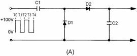
Figure 4-45A. - Basic step counter and waveforms.
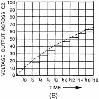
Figure 4-45B. - Basic step counter and waveforms.
As long as C2 has no discharge path, the voltage across its terminals increases
with each successive step until it is equal in amplitude to the applied pulse. The
voltage across C2 could be applied to a blocking-oscillator circuit to cause the
oscillator to pulse after a certain amount of voltage is applied to it.
The circuit in figure 4-46, (view A) and (view B), may be used as a frequency
divider. When used in this manner, Q1 is used as a single-swing blocking oscillator
that is triggered when the voltage across C2 becomes great enough to forward bias
Q1. At other times, the transistor is cut off by the bias voltage developed in the
section of R2 that is between the ground and the slide.
4-51
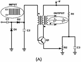
Figure 4-46A. - Step counter as a frequency divider and waveforms.
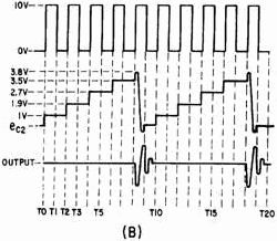
Figure 4-46B. - Step counter as a frequency divider and waveforms.
The action of the counter can best be understood by referring back to figure
4-45. Assume C2 is 10 times larger than C1 and the peak voltage is 10 volts. C1
will assume 9/10 of the positive input voltage at T0, while C2 will assume only
1/10, or 1 volt in this example. At T1 the input will drop in a negative direction
and D2 will be cut off. The cathode of D1 will become more negative than its anode
and conduct, discharging C1. The charge on C2 will remain at 1 volt because it has
no discharge path. At T2 the second pulse will be applied. The 1-volt charge on
C2 will oppose the 10 volts of the second pulse, and the applied voltage for the
capacitors to charge will be 9 volts. C2 will again charge 10 percent, or 0.9 volt.
This is in addition to the initial charge of volt. At the end of the second pulse,
the voltage on C2 will be 1.9 volts. At T3 the third pulse will be 10 volts, but
1.9 volts will oppose it. Therefore, the applied
4-52
voltage will be 10 - 1.9 volts, or 8.1 volts. C2 will charge to 10 percent of
8.1 volts, or .81 volt. The voltage on C2 will become 1 + .9 + .81, or 2.71 volts.
Successive input pulses will raise C2 by 10 percent of the remaining voltage toward
10 volts until the blocking oscillator works. If the oscillator bias is set so that
Q1 begins conduction at 3.8 volts, this will continue until 3.8 volts is exceeded.
Since the fourth step is 3.5 volts and the fifth is 4.1 volts, the 3.8-volt level
is crossed at the fifth step. If the oscillator goes through 1 cycle of operation
every fifth step and C2 is discharged at this point, this circuit would be a 5-
to-1 divider.
The circuit can be made to divide by 3, 4, or some other value by setting the
bias at a different level. For example, if the bias is set at 2.9 volts, conduction
will occur at the fourth step, making it a 4-to-1 divider.
The counting stability of the step counter is dependent upon the exponential
charging rate of capacitor C2. As C2 increases to higher steps, the voltage increments
are less and less. If the ratio becomes too great, the higher steps become almost
indiscernible. For this reason, accuracy decreases as the ratio increases. When
you desire to count by a large number, 24 for example, a 6-to-1 counter and a 4-
to-1 counter are connected in cascade (series). a more stable method of counting
24 would be to use a 2:1, 3:1, 4:1 counter connected in cascade. Most step counters
operate on a ratio of 5 to 1 or less.
Q27. What is the difference between a positive counter and a step
counter?
Summary
This chapter has presented information on wave shaping. The information that
follows summarizes the important points of this chapter.
A LIMITER is a device which limits or prevents some part of
a waveform from exceeding a specified value.
In a Series LIMITER, the diode is in series with the output.
It can limit either the negative or positive alternation of the input signal.
In a Series-Positive LIMITER, the diode is in series with the
output which is taken across the resistor. It removes the positive alternation of
the input signal.
In a Series-Positive LIMITER WITH BIAS, the bias potential will
either aid or oppose the flow of current. When aiding forward bias, only a portion
of the positive input pulse is removed. When the bias aids the reverse bias, all
of the positive and a portion of the negative pulse is removed.
4-53
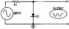
The Series-Negative LIMITER limits the negative portion of the
input pulse. The difference between a series-negative limiter and a series-positive
limiter is that the diode is reversed in the negative limiter.
A Series-Negative LIMITER with bias is the same as the series-positive
limiter with bias, but the outputs are opposite. When bias aids forward bias, only
a portion of the negative input is removed. When bias aids reverse bias, all of
the negative and a portion of the positive input is removed.
4-54
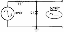
In a PARALLEL LIMITER, a resistor and diode are connected in
series with the input signal. The output is taken across the diode.
In the PARALLEL-Positive LIMITER, the positive portion of the
input signal is limited when the diode conducts.
The PARALLEL-Negative LIMITER diode is reversed from that of
the parallel positive limiter to limit only a portion of the negative input signal.
The DUAL-DIODE LIMITER combines the parallel negative limiter
with negative bias (reverse bias) and the parallel positive limiter with positive
bias (reverse bias). It will remove parts of the positive and negative input signal.
4-55
A CLAMPING Circuit effectively clamps or ties down the upper
or lower extremity of a waveform to a fixed dc potential. Clamping does not change
the amplitude or shape of the input waveform.
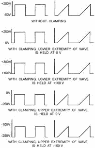
A Positive CLAMPER will clamp the lower extremity of the input
waveform to a dc potential of
0 volts.
4-56
A Negative CLAMPER will clamp the upper extremity of the input
waveform to a dc potential of 0 volts.
A Common-Base Transistor CLAMPER clamps the collector voltage
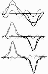
to a reference level. a waveform other than a sine wave is called a COMPLEX WAVE.
If the odd harmonics of a sine wave are added algebraically, the result is a
square wave. a PERFECT SQUARE WAVE is composed of an infinite number of odd harmonics
in phase with the fundamental wave.
4-57
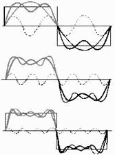
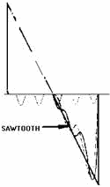
A SAWTOOTH WAVE is made up of different harmonics, both odd
and even.
A PEAKED WAVE is made up of odd harmonics that are in phase
and out of phase with the fundamental.
4-58
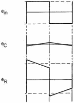
INTEGRATION takes place in an RC circuit with the output taken
across the capacitor. The amount of integration is dependent upon the time constant
of the circuit. Full integration takes place when the time constant of the RC circuit
is at least 10 times greater than the duration of the input pulse. An RL circuit
is also used as an integration circuit. The output is taken across the resistor
and the time constant of the circuit is 10 times greater than the input pulse.
4-59
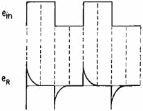
DIFFERENTIATION is the opposite of integration. In the differentiator,
the output is taken across the resistor. Full differentiation takes place when the
time constant of the circuit is 1/10 that of the input pulse.
A COUNTING Circuit receives uniform pulses, representing units
to be counted, and produces a voltage output proportional to its frequency.
ANSWERS to QUESTION Q1. Through Q27.
A1. Negative.
A2. Positive.
A3. Biasing.
A4. The diode.
A5. Conducting, cutoff.
A6. Short time constant.
A7. Long time constant.
A8. Most negative.
A9. Positive potential.
A10. Positive clamper with negative bias.
A11. Most positive.
A12. Negative potential.
A13. Positive bias.
A14. -5 volts.
4-60
A15. It is composed of an infinite number of odd harmonics in phase
with the fundamental.
A16. It is composed of odd harmonics some of which are out phase
with the fundamental.
A17. All the odd harmonics are in phase with the fundamental in the
square wave. This is not true of the odd harmonics in the peaked wave.
A18. The time constant is long and the output is taken across the
capacitor in an RC circuit.
A19. a pure sine wave cannot be integrated; it contains no harmonics.
A20. The ability of the inductor to oppose a change in current.
A21. The time-constant value of a long time constant-circuit is 10
times the value of the input pulse duration. The short time-constant circuit has
a time constant of 1/10 of the pulse duration.
A22. a more complete integration of the waveform would result from
the long time constant.
A23. In an RC circuit the output is taken across the resistor. In
the RL circuit the output is taken across the inductor.
A24. Frequency counters or frequency dividers.
A25. The frequency of the voltage input.
A26. To provide a quick discharge path for C1.
A27. The load resistor in a positive counter is replaced by a capacitor
in a step counter.
4-61
|