NEETS Module 9 − Introduction to Wave− Generation and Wave−Shaping
Pages i,
1−1,
1−11,
1−21,
1−31,
1−41,
2−1,
2−11,
2−21,
2−31,
3−1,
3−11,
3−21,
3−31,
3−41,
3−51,
4−1,
4−11,
4−21,
4−31,
4−41,
4−51, Index
| - |
Matter, Energy,
and Direct Current |
| - |
Alternating Current and Transformers |
| - |
Circuit Protection, Control, and Measurement |
| - |
Electrical Conductors, Wiring Techniques,
and Schematic Reading |
| - |
Generators and Motors |
| - |
Electronic Emission, Tubes, and Power Supplies |
| - |
Solid-State Devices and Power Supplies |
| - |
Amplifiers |
| - |
Wave-Generation and Wave-Shaping Circuits |
| - |
Wave Propagation, Transmission Lines, and
Antennas |
| - |
Microwave Principles |
| - |
Modulation Principles |
| - |
Introduction to Number Systems and Logic Circuits |
| - |
- Introduction to Microelectronics |
| - |
Principles of Synchros, Servos, and Gyros |
| - |
Introduction to Test Equipment |
| - |
Radio-Frequency Communications Principles |
| - |
Radar Principles |
| - |
The Technician's Handbook, Master Glossary |
| - |
Test Methods and Practices |
| - |
Introduction to Digital Computers |
| - |
Magnetic Recording |
| - |
Introduction to Fiber Optics |
| Note: Navy Electricity and Electronics Training
Series (NEETS) content is U.S. Navy property in the public domain. |
PARALLEL-Positive LIMITER WITH BIAS. - Figure 4-10, view (A),
shows the schematic diagram of a PARALLEL-Positive LIMITER WITH Negative BIAS. The
diode is forward biased and conducts without an input signal. D1 is essentially
a short circuit. The voltage at the output terminals is -4 volts.
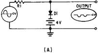
Figure 4-10A. - Parallel limiter with negative bias.
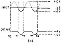
Figure 4-10B. - Parallel limiter with negative bias.
As the positive alternation of the input signal is applied to the circuit,
the diode remains forward biased and limits the entire positive alternation, as
shown in view (B). As the signal goes in a negative direction Oust before T1), the
diode remains forward biased (limiting is still present) until the input signal
4-11
exceeds -4 volts (T1). D1 becomes reverse biased as the anode becomes more negative
than the cathode. While the input signal is more negative than the -4 volts of the
bias battery (T1 to T2), the diode is reverse biased and remains cut off. The output
follows the input signal from T1 to T2. At all other times during that cycle, the
diode is forward biased and limiting occurs. This circuit is called a parallel-positive
limiter with negative bias because the positive output is limited and the bias in
the circuit is negative with reference to ground. Limiting takes place at all points
more positive than -4 volts.
The circuit shown in figure 4-11, view (A), is a PARALLEL-Positive LIMITER WITH
Positive BIAS. The positive terminal of the battery is connected to the cathode
of the diode. This causes the diode to be reverse biased at all times except when
the input signal is more positive than the bias voltage (T1 to T2), as shown in
view (B).
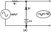
Figure 4-11A. - Parallel-positive Limiter with positive bias.
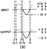
Figure 4-11B. - Parallel-positive Limiter with positive bias.
As the positive alternation of the input signal is applied (T0), the output voltage
follows the input signal. From T1 to T2 the input signal is more positive than +
4 volts. The diode is forward biased and conducts. At this time the output voltage
equals the bias voltage and limiting takes place. From T2 to T4 of the input signal,
the diode is reverse biased and does not conduct. The output signal follows the
input signal and no limiting takes place.
4-12
This circuit is called a parallel-positive limiter with positive bias because
limiting takes place in the positive alternation and positive bias is used on the
diode.
Parallel-Negative Limiter
a PARALLEL-Negative LIMITER is shown in view (A) of figure 4-12. Notice the similarity
of the parallel-negative limiter and the parallel-positive limiter shown in view
(A) of figure 4-9. From T0 to T1 of the input signal, the diode is reverse biased
and does not conduct, as shown in view (B) of figure 4-12. The output signal follows
the input signal and the positive alternation is not limited.
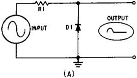
Figure 4-12A. - Parallel-negative limiter.
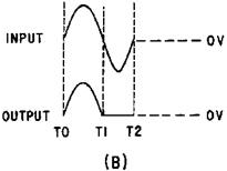
Figure 4-12B. - Parallel-negative limiter.
During the negative alternation of the input signal (T1 to T2), the diode is
forward biased and conducts. The relatively low forward bias of D1 develops a very
small voltage and, therefore, limits the output to nearly 0 volts. a voltage is
developed across the resistor as current flows through the resistor and diode.
4-13
PARALLEL-Negative LIMITER WITH BIAS. - The circuit shown in
figure 4-13, view (A), is a parallel-negative limiter with negative bias. With no
input, the battery maintains D1 in a reverse-bias condition. D1 cannot conduct until
its cathode is more negative than its anode. D1 acts as an open until the input
signal dips below -4 volts at T2 in view (B). At T2 the input signal becomes negative
enough to forward bias the diode, D1 conducts and acts like a short, and the output
is limited to the -4 volts from the battery from T2 to T3. Between T3 and T4 the
diode is again reverse biased. The output signal follows the input signal and no
limiting occurs.
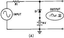
Figure 4-13A. - Parallel-negative limiter with negative bias.
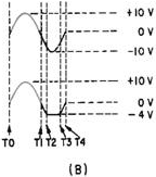
Figure 4-13B. - Parallel-negative limiter with negative bias.
Figure 4-14, view (A), shows a parallel-negative limiter with positive bias.
The operation is similar to those circuits already explained. Limiting occurs when
the diode conducts. No limiting occurs when the diode is reverse biased. In this
circuit, the bias battery provides forward bias to the diode without an input signal.
The output is at +4 volts, except where the input goes above +4 volts (T1 to T2),
as shown in view (B). The parts of the signal more negative than +4 volts are limited.
4-14
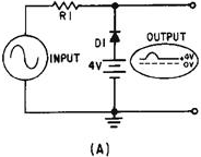
Figure 4-14A. - Parallel-negative limiter with positive bias.
Figure 4-14B. - Parallel-negative limiter with positive bias.
Q4. What component is in parallel with the output in a parallel limiter?
Q5. What is the condition of the diode in a series limiter when an
output is developed? In a parallel limiter?
DUAL-DIODE LIMITER
The last type of limiter to be discussed in this chapter is the DUAL-DIODE LIMITER,
shown in figure 4-15, view (A). This limiter combines a parallel-negative limiter
with negative bias (D1 and B1) and a parallel-positive limiter with positive bias
(D2 and B2). Parts of both the positive and negative alternations are removed in
this circuit. Each battery aids the reverse bias of the diode in its circuit; the
circuit has no current flow with no input signal. When the input signal is below
the value of the biasing batteries, both D1 and D2 are reverse biased. With D1 and
D2 reverse biased, the output follows the input. When the input signal becomes more
positive than +20 volts (view (B)), D2 conducts and limits the output to +20 volts.
When the input signal becomes more negative than -20 volts, D1 conducts and limits
the output to this, value. When neither diode conducts, the output follows the input
waveform.
4-15
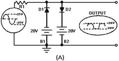
Figure 4-15A. - Dual-diode limiter.
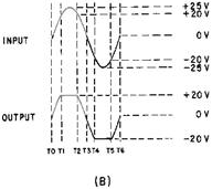
Figure 4-15B. - Dual-diode limiter.
CLAMPERS
Certain applications in electronics require that the upper or lower extremity
of a wave be fixed at a specific value. In such applications, a CLAMPING (or CLAMPER)
circuit is used. a clamping circuit clamps or restrains either the upper or lower
extremity of a waveform to a fixed dc potential. This circuit is also known as a
Direct-CURRENT RESTORER or a Base-LINE STABILIZER. Such circuits are used in test
equipment, radar systems, electronic countermeasure systems, and sonar systems.
Depending upon the equipment, you could find negative or positive clampers with
or without bias. Figure 4-16, views (A) through (E), illustrates some examples of
waveforms created by clampers. However, before we discuss clampers, we will review
some relevant points about series RC circuits.
4-16
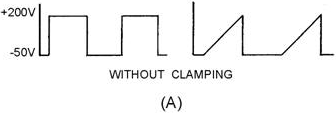
Figure 4-16A. - Clamping waveforms. WITHOUT CLAMPING.
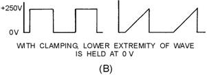
Figure 4-16B. - Clamping waveforms. WITH CLAMPING, LowER EXTREMITY of WAVE Is
HELD AT 0V.
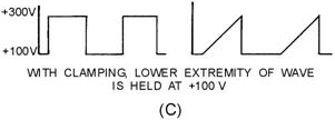
Figure 4-16C. - Clamping waveforms. WITH CLAMPING, LowER EXTREMITY of WAVE Is
HELD AT +100 V.
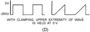
Figure 4-16D. - Clamping waveforms. WITH CLAMPING, Upper EXTREMITY of WAVE Is
HELD AT 0V.
4-17
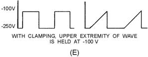
Figure 4-16E. - Clamping waveforms. WITH CLAMPING, Upper EXTREMITY of WAVE Is
HELD AT
-100 V.
Series RC Circuits
Series RC circuits are widely used for coupling signals from one stage to another.
If the time constant of the coupling circuit is comparatively long, the shape of
the output waveform will be almost identical to that of the input. However, the
output dc reference level may be different from that of the input. Figure 4-17,
view (A), shows a typical RC coupling circuit in which the output reference level
has been changed to 0 volts. In this circuit, the values of R1 and C1 are chosen
so that the capacitor will charge (during T0 to T1) to 20 percent of the applied
voltage, as shown in view (B). With this in mind, let's consider the operation of
the circuit.
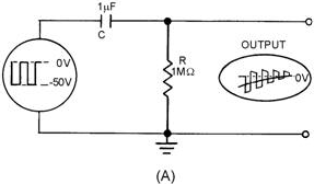
Figure 4-17A. - RC coupling.
4-18
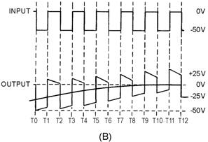
Figure 4-17B. - RC coupling.
At T0 the input voltage is -50 volts and the capacitor begins charging. At the
first instant the voltage across C is 0 and the voltage across R is -50 volts. As
C charges, its voltage increases. The voltage across R, which is the output voltage,
begins to drop as the voltage across C increases. At T1 the capacitor has charged
to 20 percent of the -50 volts input, or -10 volts. Because the input voltage is
now 0 volts, the capacitor must discharge. It discharges through the low impedance
of the signal source and through R, developing +10 volts across R at the first instant.
C discharges 20 percent of the original 10-volt charge from T1 to T2. Thus, C discharges
to +8 volts and the output voltage also drops to 8 volts.
At T2 the input signal becomes -50 volts again. This -50 volts is in series opposition
to the 8-volt charge on the capacitor. Thus, the voltage across R totals -42 volts
(-50 plus +8 volts). Notice that this value of voltage (-42 volts) is smaller in
amplitude than the amplitude of the output voltage which occurred at to (-50 volts).
Capacitor C now charges from +8 to +16 volts. If we were to continue to follow the
operation of the circuit, we would find that the output wave shape would become
exactly distributed around the 0-volt reference point. At that time the circuit
operation would have reached a stable operating point. Note that the output wave
shape has the same amplitude and approximately the same shape as the input wave
shape, but now "rides" equally above and below 0 volts. Clampers use this RC time
so that the input and output waveforms will be almost identical, as shown from T11
to T12.
Positive-DIODE CLAMPERS
Figure 4-18, view (A), illustrates the circuit of a positive-diode clamper. Resistor
R1 provides a discharge path for C1. This resistance is large in value so that the
discharge time of C1 will be long compared to the input pulse width. The diode provides
a fast charge path for C1. After C1 becomes charged it acts as a voltage source.
The input wave shape shown in view (B) is a square wave and varies between +25 volts
and -25 volts. Compare each portion of the input wave shape with the corresponding
output wave shape. Keep Kirchhoff's law in mind: The algebraic sum of the voltage
drops around a closed loop is 0 at any instant.
4-19
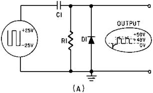
Figure 4-18A. - Positive damper and waveform.
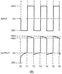
Figure 4-18B. - Positive damper and waveform.
At T0 the -25 volt input signal appears across R1 and D1 (the capacitor is a
short at the first instant). The initial voltage across R1 and D1 causes a voltage
spike in the output. Because the charge time of C1 through D1 is almost instantaneous,
the duration of the pulse is so short that it has only a negligible effect on the
output. The -25 volts across D1 makes the cathode negative with respect to the anode
and the diode conducts heavily. C1 quickly charges through the small resistance
of D1. As the voltage across C1 increases, the output voltage decreases at the same
rate. The voltage across C1 reaches -25 volts and the output is at 0 volts.
4-20
|