NEETS Module 9 − Introduction to Wave− Generation and Wave−Shaping
Pages i,
1−1,
1−11,
1−21,
1−31,
1−41,
2−1,
2−11,
2−21,
2−31,
3−1,
3−11,
3−21,
3−31,
3−41,
3−51,
4−1,
4−11,
4−21,
4−31,
4−41,
4−51, Index
| - |
Matter, Energy,
and Direct Current |
| - |
Alternating Current and Transformers |
| - |
Circuit Protection, Control, and Measurement |
| - |
Electrical Conductors, Wiring Techniques,
and Schematic Reading |
| - |
Generators and Motors |
| - |
Electronic Emission, Tubes, and Power Supplies |
| - |
Solid-State Devices and Power Supplies |
| - |
Amplifiers |
| - |
Wave-Generation and Wave-Shaping Circuits |
| - |
Wave Propagation, Transmission Lines, and
Antennas |
| - |
Microwave Principles |
| - |
Modulation Principles |
| - |
Introduction to Number Systems and Logic Circuits |
| - |
- Introduction to Microelectronics |
| - |
Principles of Synchros, Servos, and Gyros |
| - |
Introduction to Test Equipment |
| - |
Radio-Frequency Communications Principles |
| - |
Radar Principles |
| - |
The Technician's Handbook, Master Glossary |
| - |
Test Methods and Practices |
| - |
Introduction to Digital Computers |
| - |
Magnetic Recording |
| - |
Introduction to Fiber Optics |
| Note: Navy Electricity and Electronics Training
Series (NEETS) content is U.S. Navy property in the public domain. |
advantage of the common-emitter configuration is that the medium resistance range
of the input and output simplifies the job of impedance matching.
Q-6. What type of feedback aids an input signal?
Q-7. What are the two methods used for feedback coupling?
Q-8. Which oscillator uses a tickler coil for feedback?
Q-9. Which oscillator uses a tapped inductor for feedback?
Q-10. Which oscillator uses tapped capacitors for feedback?
Q-11. What are the three basic configurations of transistor oscillators?
Oscillator Circuits
Oscillators may be classified by name, such as Armstrong, Hartley, Colpitts,
or by the manner in which dc power is applied. An oscillator in which dc power is
supplied to the transistor through the tank circuit, or a portion of the tank circuit,
is said to be Series FED. An oscillator which receives its dc power for the transistor
through a path separate and parallel to the tank circuit is said to be PARALLEL
FED OR Shunt FED. All the oscillators in this chapter can be constructed either
way, series or shunt fed. The construction depends on the characteristics of the
oscillator circuit the designer is interested in.
A Series-FED, Tuned-Collector ARMSTRONG Oscillator is illustrated in figure 2-9,
view (A). The dc path is from the negative side (ground) of VCC
through RE, Q1, T1, and back to the positive side of VCC.
The figure clearly illustrates that both the ac and dc components flow through the
tank circuit.
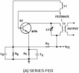
Figure 2-9A. - Series- and shunt-fed, tuned-collector Armstrong oscillators.
Series-FED.
2-11
By modifying the circuit slightly, it becomes a Shunt-FED, Tuned-Collector ARMSTRONG
Oscillator as shown in view (B). The dc component flows from ground through RE
to Q1 to positive VCC. The dc is blocked from the tank circuit by capacitor
C2. Only the ac component flows in the tank circuit.
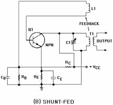
Figure 2-9B. - Series- and shunt-fed, tuned-collector Armstrong oscillators.
Shunt-FED.
The function of an oscillator is to produce a sinusoidal waveshape of a specific
frequency and amplitude. In doing so, the stability of an oscillator is very important.
Depending on its application, an oscillator may be required to have either good
frequency stability or amplitude stability; in many circumstances, both are required.
Of the two, good frequency stability is usually considered more important.
Frequency STABILITY
The Frequency STABILITY of an oscillator is a measure of the degree to which
a constant frequency output is approached. The better the frequency stability, the
closer the output will be to a constant frequency.
Frequency INSTABILITY (variations above and below the desired output frequency)
may be caused by transistor characteristics or by variations in the external circuit
elements.
As stated before, when output power is not of prime importance, transistor oscillators
may be biased class a to ensure stability and minimize distortion. When this is
done, the dc operating point established by the power supply is chosen so that the
operation of the transistor oscillator occurs over the most linear portion of the
transistor's characteristic curve. When the operation of the circuit falls into
the nonlinear portion of the characteristic curve, the transistor's parameters (voltages
and currents) vary. These parameters are basic to the stable frequency of the transistor
oscillator. Operating frequency variations may occur with changes in these bias
voltages. Thus, a constant supply voltage is a prime requirement for good frequency
stability.
The use of a common bias source for both collector and emitter electrodes results
in a relatively constant ratio of the two voltages. In effect, a change in one voltage
is somewhat counteracted by the change in the other. This counteraction takes place
because an increase in collector voltage causes an
2-12
increase in the oscillating frequency, and an increase in emitter voltage causes
a decrease in the oscillating frequency. This is a result of the change in capacitance
between the junctions of the transistor. However, a common bias source does not
completely compensate since the effects on other circuit parameters of each bias
voltage differ.
Just as in any transistor circuit, changes in the transistor operating point
and changes in temperature are encountered in the transistor oscillator. The effects
of changes in temperature are to cause collector current to increase if the transistor
is not stabilized. The increase in collector current can be prevented by reducing
the forward bias.
Amplitude STABILITY
The Amplitude STABILITY of a transistor oscillator indicates the amount by which
the actual output amplitude varies from the desired output amplitude.
The same parameters (voltages and currents) that affect frequency stability also
affect amplitude stability. Output amplitude may be kept relatively constant by
ensuring that the feedback is large enough that the collector current is maintained
at the proper level. Feedback used in this manner makes the output voltage directly
proportional to the supply voltage. Thus, regulation of the supply voltage ensures
good amplitude stability.
ARMSTRONG Oscillator
The ARMSTRONG Oscillator is used to produce a sine-wave output of constant amplitude
and of fairly constant frequency within the RF range. It is generally used as a
local oscillator in receivers, as a source in signal generators, and as a radio-frequency
oscillator in the medium- and high-frequency range.
The identifying characteristics of the Armstrong oscillator are that (1) it uses
an LC tuned circuit to establish the frequency of oscillation, (2) feedback is accomplished
by mutual inductive coupling between the tickler coil and the LC tuned circuit,
and (3) it uses a class C amplifier with self-bias. Its frequency is fairly stable,
and the output amplitude is relatively constant.
Views (A), (B), and (C) shown in figure 2-10 can be used to build the basic Armstrong
oscillator. View (A) shows a conventional amplifier. R2 provides the forward bias
for Q1, C2 is a coupling capacitor, and L1 and R1 form the collector load impedance.
This is a common-emitter configuration which provides the 180-degree phase shift
between the base and collector.
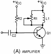
Figure 2-10A. - Basic Armstrong oscillator circuit. Amplifier
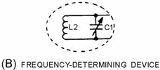
Figure 2-10B. - Basic Armstrong oscillator circuit. Frequency-Determining DEVICE.
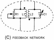
Figure 2-10C. - Basic Armstrong oscillator circuit. Feedback Network.
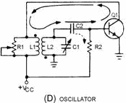
Figure 2-10D. - Basic Armstrong oscillator circuit. Oscillator.
View (B) shows the frequency-determining device composed of inductor L2 and capacitor
C1. C1 is a variable tuning capacitor which is used to adjust the resonant frequency
to the desired value.
View (C) is the feedback network which uses L1 (the collector load) as the primary
and L2 as the secondary winding of a coupling transformer to provide a 180-degree
phase shift. Variable resistor R1 controls the amount of current through L1. When
R1 is adjusted for maximum resistance, most of the current flows through L1. The
transformer now couples a maximum signal which represents a large feedback amplitude
into the tank circuit (L2, C1). If R1 is adjusted for a smaller resistance, less
current
2-14
flows through L1, and less energy is coupled to the tank circuit; therefore,
feedback amplitude decreases. R1 is normally adjusted so that the L1 current is
adequate to sustain tank oscillations.
View (D) shows the complete oscillator circuit. Connecting the feedback network
through coupling capacitor C2 to the base of Q1 forms a "closed loop" for feedback
(shown by the solid arrows). Let's verify that the feedback is regenerative. Assume
a positive signal on the base of Q1. The transistor conducts heavily when forward
biased. This current flow through L1 and R1 causes the voltage across L1 to increase.
The voltage increase is inductively coupled to L2 and inverted. This action ensures
that the voltage is positive at the base end of L2 and C1 and in phase with the
base voltage. The positive signal is now coupled through C2 to the base of Q1. The
regenerative feedback offsets the damping in the frequency-determining network and
has sufficient amplitude to provide unity circuit gain.
The circuit in view (D) has all three requirements for an oscillator: (1) amplification,
(2) a frequency- determining device, and (3) regenerative feedback. The oscillator
in this schematic drawing is a tuned- base oscillator, because the FDD is in the
base circuit. If the FDD were in the collector circuit, it would be a tuned-collector
oscillator. The circuit in view (D) is basically an Armstrong oscillator.
Refer to figure 2-10, view (D), for the following discussion of the circuit operation
of the Armstrong oscillator. When VCC is applied to the circuit. a small amount
of base current flows through R2 which sets the forward bias on Q1. This forward
bias causes collector current to flow from ground through Q1, R1, and L1 to +VCC.
The current through L1 develops a magnetic field which induces a voltage into the
tank circuit. The voltage is positive at the top of L2 and C1. At this time, two
actions occur. First, resonant tank capacitor C1 charges to this voltage; the tank
circuit now has stored energy. Second, coupling capacitor C2 couples the positive
signal to the base of Q1. With a positive signal on its base, Q1 conducts harder.
With Q1 conducting harder, more current flows through L1, a larger voltage is induced
into L2, and a larger positive signal is coupled back to the base of Q1. While this
is taking place, the frequency- determining device is storing more energy and C1
is charging to the voltage induced into L2.
The transistor will continue to increase in conduction until it reaches saturation.
At saturation, the collector current of Q1 is at a maximum value and cannot increase
any further. With a steady current through L1, the magnetic fields are not moving
and no voltage is induced into the secondary.
With no external voltage applied, C1 acts as a voltage source and discharges.
As the voltage across C1 decreases, its energy is transferred to the magnetic field
of L2. Now, let's look at C2.
The coupling capacitor, C2, has charged to approximately the same voltage as
C1. As C1 discharges, C2 discharges. The primary discharge path for C2 is through
R2 (shown by the dashed arrow). As C2 discharges, the voltage drop across R2 opposes
the forward bias on Q1 and collector current begins to decrease. This is caused
by the decreasing positive potential at the base of Q1.
A decrease in collector current allows the magnetic field of L1 to collapse.
The collapsing field of L1 induces a negative voltage into the secondary which is
coupled through C2 and makes the base of Q1 more negative. This, again, is regenerative
action; it continues until Q1 is driven into cutoff.
When Q1 is cut off, the tank circuit continues to flywheel, or oscillate. The
flywheel effect not only produces a sine-wave signal, but it aids in keeping Q1
cut off. Without feedback, the oscillations of L2 and C1 would dampen out after
several cycles.
To ensure that the amplitude of the signal remains constant, regenerative feedback
is supplied to the tank once each cycle, as follows: As the voltage across C1 reaches
maximum negative, C1 begins discharging toward 0 volts. Q1 is still below cutoff.
C1 continues to discharge through 0 volts and becomes positively charged. The tank
circuit voltage is again coupled to the base of Q1, so the base voltage becomes
positive and allows collector current to flow. The collector current creates a magnetic
2-15
field in L1, which is coupled into the tank. This feedback action replaces any
lost energy in the tank circuit and drives Q1 toward saturation. After saturation
is reached, the transistor is again driven into cutoff.
The operation of the Armstrong oscillator is basically this: Power applied to
the transistor allows energy to be applied to the tank circuit causing it to oscillate.
Once every cycle, the transistor conducts for a short period of time (class C operation)
and returns enough energy to the tank to ensure a constant amplitude output signal.
Class C operation has high efficiency and low loading characteristics. The longer
Q1 is cut off, the less the loading on the frequency-determining device.
Figure 2-11 shows a tuned-base Armstrong oscillator as you will probably see
it. R3 has been added to improve temperature stability. Bypass capacitor C3 prevents
degeneration. C4 is an output coupling capacitor, and impedance-matching transformer
T2 provides a method of coupling the output signal. T2 is usually a loosely coupled
RF transformer which reduces undesired reflected impedance from the load back to
the oscillator.
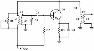
Figure 2-11. - Tuned-base Armstrong oscillator.
The Armstrong oscillator is an example of how a class C amplifier can produce
a sine-wave output that is not distorted. Although class C operation is nonlinear
and many harmonic frequencies are generated, only one frequency receives enough
gain to cause the circuit to oscillate. This is the frequency of the resonant tank
circuit. Thus, high efficiency and an undistorted output signal can be obtained.
The waveforms in figure 2-12 illustrate the relationship between the collector
voltage and collector current. Notice that collector current (IC) flows for only
a short time during each cycle. While the tank circuit is oscillating (figure 2-11),
L2 acts as the primary of the transformer and L1 acts as the secondary. The signal
from the tank is, therefore, coupled through T1 to coupling capacitor C4, and the
output voltage across L4 is a sine wave.
2-16
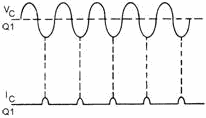
Figure 2-12. - Collector current and voltage waveforms of a class C oscillator.
HARTLEY Oscillator
The HARTLEY Oscillator is an improvement over the Armstrong oscillator. Although
its frequency stability is not the best possible of all the oscillators, the Hartley
oscillator can generate a wide range of frequencies and is very easy to tune. The
Hartley will operate class C with self-bias for ordinary operation. It will operate
class a when the output waveform must be of a constant voltage level or of a linear
waveshape. The two versions of this oscillator are the series-fed and the shunt-fed.
The main difference between the Armstrong and the Hartley oscillators lies in the
design of the feedback (tickler) coil. a separate coil is not used. Instead, in
the Hartley oscillator, the coil in the tank circuit is a split inductor. Current
flow through one section induces a voltage in the other section to develop a feedback
signal.
Series-Fed Hartley Oscillator
One version of a Series-FED HARTLEY Oscillator is shown in figure 2-13. The tank
circuit consists of the tapped coil (L1 and L2) and capacitor C2. The feedback circuit
is from the tank circuit to the base of Q1 through the coupling capacitor C1. Coupling
capacitor C1 prevents the low dc resistance
of L2 from placing a short across the emitter-to-base junction and resistor RE.
Capacitor C3 bypasses the sine-wave signal around the battery, and resistor RE
is used for temperature stabilization to prevent thermal runaway. Degeneration is
prevented by CE in parallel with RE. The amount of bias is determined by the
values of RB, the emitter-to-base resistance, the small amount of dc resistance
of coil L1, and the resistance of RE.
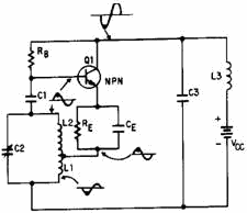
Figure 2-13. - Series-fed, tuned-base Hartley oscillator.
2-17
When a voltage is applied to the circuit, current from the battery flows through
coil L1 and to the emitter through RE. Current then flows from the emitter to the
collector and back to the battery. The surge of current through coil L1 induces
a voltage in coil L2 to start oscillations within the tank circuit.
When current first starts to flow through coil L1, the bottom of L1 is negative
with respect to the top of L2. The voltage induced into coil L2 makes the top of
L2 positive. As the top of L2 becomes positive, the positive potential is coupled
to the base of Q1 by capacitor C1. a positive potential on the base results in an
increase of the forward bias of Q1 and causes collector current to increase. The
increased collector current also increases the emitter current flowing through coil
L1. Increased current through L1 results in more energy being supplied to the tank
circuit, which, in turn, increases the positive potential at the top of the tank
(L2) and increases the forward bias of Q1. This action continues until the rate
of current change through coil L1 can no longer increase. The current through coil
L1 and the transistor cannot continue increasing indefinitely, or the coil and transistor
will burn up. The circuit must be designed, by proper selection of the transistor
and associated parts, so that some point is reached when the current can no longer
continue to increase. At this point C2 has charged to the potential across L1 and
L2. This is shown as the heavy dot on the base waveform. As the current through
L1 decreases, the voltage induced in L2 decreases. The positive potential across
the tank begins to decrease and C2 starts discharging through L1 and L2. This action
maintains current flow through the tapped coil and causes a decrease in the forward
bias of Q1. In turn, this decrease in the forward bias of Q1 causes the collector
and emitter current to decrease. At the instant the potential across the tank circuit
decreases to 0, the energy of the tank circuit is contained in the magnetic field
of the coil. The oscillator has completed a half cycle of operation.
Next, the magnetic field around L2 collapses as the current from C2 stops. The
action of the collapsing magnetic field causes the top of L2 to become negative
at this instant. The negative charge causes capacitor C2 to begin to charge in the
opposite direction. This negative potential is coupled to the base of Q1, opposing
its forward bias. Most transistor oscillators are operated class A; therefore, the
positive and negative signals applied to the base of Q1 will not cause it to go
into saturation or cutoff. When the tank circuit reaches its maximum negative value,
the collector and the emitter currents will still be present but at a minimum value.
The magnetic field will have collapsed and the oscillator will have completed 3/4
cycle.
At this point C2 begins to discharge, decreasing the negative potential at the
top of L2 (potential will swing in the positive direction). As the negative potential
applied to the base of Q1 decreases, the opposition to the forward bias also decreases.
This, in effect, causes the forward bias to begin increasing, resulting in increased
emitter current flowing through L1. The increase in current through L1 causes additional
energy to be fed to the tank circuit to replace lost energy. If the energy lost
in the tank is replaced with an equal or larger amount of energy, oscillations will
be sustained. The oscillator has now completed 1 cycle and will continue to repeat
it over and over again.
Shunt-Fed Hartley Oscillator
A version of a Shunt-FED HARTLEY Oscillator is shown in figure 2-14. The parts
in this circuit perform the same basic functions as do their counterparts in the
series-fed Hartley oscillator. The difference between the series-fed and the shunt-fed
circuit is that dc does not flow through the tank circuit. The shunt-fed circuit
operation is essentially the same as the series-fed Hartley oscillator. When voltage
is applied to the circuit, Q1 starts conducting. As the collector current of Q1
increases, the change
(increase) is coupled through capacitor C3 to the tank circuit, causing it to
oscillate. C3 also acts as an isolation capacitor to prevent dc from flowing through
the feedback coil. The oscillations at the collector
will be coupled through C3 (feedback) to supply energy lost within the tank.
2-18
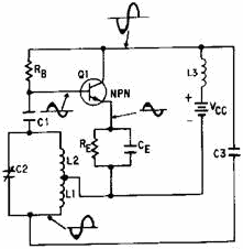
Figure 2-14. - Shunt-fed, tuned-base Hartley oscillator.
Q-12. What is the main difference between the Armstrong oscillator
and the Hartley oscillator?
Q-13. What is the difference between the series-fed and the shunt-fed
Hartley oscillator?
COLPITTS Oscillator
Both the Armstrong and the Hartley oscillators have a tendency to be unstable
in frequency because of junction capacitance. In comparison, the COLPITTS Oscillator
has fairly good frequency stability, is easy to tune, and can be used for a wide
range of frequencies. The large value of split capacitance is in parallel with the
junctions and minimizes the effect on frequency stability.
The Colpitts oscillator is very similar to the shunt-fed Hartley oscillator,
except that two capacitors are used in the tank circuit instead of a tapped coil
(figure 2-15). The Hartley oscillator has a tap between two coils, while the Colpitts
has a tap between two capacitors. You can change the frequency of the Colpitts either
by varying the inductance of the coil or by varying the capacitance of the two capacitors
in the tank circuit. Notice that no coupling capacitor is used between the tank
circuit and the base of Q1. Capacitors C1 and C2 of the tank circuit are in parallel
with the input and the output interelement capacitance (capacitance between emitter,
base, and collector) of the transistor. Thus the input and the output capacitive
effect can be minimized on the tank circuit and better frequency stability can be
obtained than with the Armstrong or the Hartley oscillator.
2-19
Figure 2-15. - Colpitts oscillator.
Figure 2-16 shows a common-base Colpitts oscillator using a pnp transistor as
the amplifying device. Notice in this version of the Colpitts oscillator that regenerative
feedback is obtained from the tank circuit and applied to the emitter. Base bias
is provided by resistor RB and RF. Resistor R C is the collector load
resistor. Resistor RE develops the input signal and also acts as
the emitter swamping resistor. The tuned circuit consists of C1 and C2 in parallel
with the primary winding of transformer T1. The voltage developed across C2 is the
feedback voltage. Either or both capacitors may be adjusted to control the frequency.
In the common-base configuration there is no phase difference between the signal
at the collector and the emitter signal. Therefore, the phase of the feedback signal
does not have to be changed. When the emitter swings negative, the collector also
swings negative and C2 charges negatively at the junction of C1 and C2. This negative
charge across C2 is fed back to the emitter. This increases the reverse bias on
Q1. The collector of Q1 becomes more negative and C2 charges to a negative potential.
This feedback effect continues until the collector of Q1 is unable to become any
more negative. At that time the primary of T1 will act as a source because of normal
tank circuit operation. As its field collapses, the tank potential will reverse
and C1 and C2 will begin to discharge. As C2 becomes less negative, the reverse
bias on Q1 decreases and its collector voltage swings in the positive direction.
C1 and C2 will continue to discharge and then charge in a positive direction. This
positive-going voltage across C2 will be fed back to the emitter as regenerative
feedback. This will continue until the field around the primary of T1 collapses.
At that time the collector of Q1 will be at a maximum positive value. C1 and C2
will begin to discharge and the potential at their junction will become less positive.
This increases the reverse bias on Q1 and drives the collector negative, causing
C1 and C2 to charge in a negative direction and to repeat the cycle.
2-20
|