NEETS Module 9 − Introduction to Wave− Generation and Wave−Shaping
Pages i,
1−1,
1−11,
1−21,
1−31,
1−41,
2−1,
2−11,
2−21,
2−31,
3−1,
3−11,
3−21,
3−31,
3−41,
3−51,
4−1,
4−11,
4−21,
4−31,
4−41,
4−51, Index
| - |
Matter, Energy,
and Direct Current |
| - |
Alternating Current and Transformers |
| - |
Circuit Protection, Control, and Measurement |
| - |
Electrical Conductors, Wiring Techniques,
and Schematic Reading |
| - |
Generators and Motors |
| - |
Electronic Emission, Tubes, and Power Supplies |
| - |
Solid-State Devices and Power Supplies |
| - |
Amplifiers |
| - |
Wave-Generation and Wave-Shaping Circuits |
| - |
Wave Propagation, Transmission Lines, and
Antennas |
| - |
Microwave Principles |
| - |
Modulation Principles |
| - |
Introduction to Number Systems and Logic Circuits |
| - |
- Introduction to Microelectronics |
| - |
Principles of Synchros, Servos, and Gyros |
| - |
Introduction to Test Equipment |
| - |
Radio-Frequency Communications Principles |
| - |
Radar Principles |
| - |
The Technician's Handbook, Master Glossary |
| - |
Test Methods and Practices |
| - |
Introduction to Digital Computers |
| - |
Magnetic Recording |
| - |
Introduction to Fiber Optics |
| Note: Navy Electricity and Electronics Training
Series (NEETS) content is U.S. Navy property in the public domain. |
So far, the basic flip-flop has used only PNP transistors. It could have just
as easily used NPN transistors. The functional operation would not change; only
the polarities required for conduction and cutoff change. As a technician, you may
see either type of transistor used, NPN or PNP. a symbolic block diagram is sometimes used to avoid confusion about voltage polarities.
A special kind of block diagram has been adopted as a standard symbol for the
flip-flop and is shown in figures 3-25 and 3-26. The two inputs are represented
by the lines on the left and the outputs by the lines on the right. InputS to a
flip-flop are S (SET) and C (CLEAR) and OutputS from a flip-flop are "1" and "0."
a trigger pulse applied to the SET input causes the "1" output to be a positive
or negative voltage, depending on the type of transistor. At the same time, the
"0" output equals 0 volts. This condition is called the SET STATE.
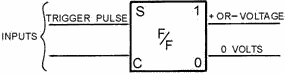
Figure 3-25. - Flip-flop (SET state).
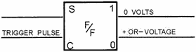
Figure 3-26. - Flip-flop (CLEAR state).
If a trigger pulse is applied to the CLEAR input, a positive or negative voltage
is produced at the "0" output. The "1" output goes to 0 volts. This condition is
called the CLEAR STATE, as shown in figure 3-26.
To determine what state the flip-flop is in, you can measure either the "1" or
the "0" output. Measuring 0 volts at the "1" output indicates that the flip-flop
is in the CLEAR state. If the "0" output is measured, a positive or negative voltage
would also indicate that the flip-flop is in the CLEAR state. Either way, only one
reading is necessary.
In figure 3-27, the flip-flop is in the SET state prior to T0 (negative voltage
on the "1" output). Now compare the changes in output voltage at each point in time
(T0, T1, T2, and T3) with the input pulse. Studying this figure should help you
understand how the flip-flop works. The positive pulse at T0 on the CLEAR input
shifts the f/f to the CLEAR state (negative voltage at the "0" output). At T1 a
positive pulse on the SET input drives the "1" output to the SET state. At T2 a
positive pulse on the CLEAR input drives the "0" output to a CLEAR state. At T3
another positive pulse is applied to the CLEAR input. This input has no effect since
the f/f is already in the CLEAR state.
3-21
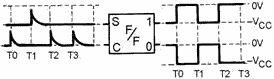
Figure 3-27. - Flip-flop with trigger pulse on SET and inputs.
Some flip-flops use a third input lead, as shown in figure 3-28. This third input
lead is called a TOGGLE (T) input. Every time a pulse is applied to the T input,
the flip-flop will change states from whatever its state was previously. The two
diodes (CR1, CR2) form a STEERING Network. This steering network directs a positive
input pulse to the saturated transistor, causing it to cut off. Negative pulses
are blocked by the diodes. Note that if NPN transistors were used, the diodes would
have to be reversed and the TOGGLE signal would have to be negative. For example,
assume that Q1 is saturated, Q2 is cut off, and a positive pulse is applied the
at T input. The input pulse will be directed to both transistors. The positive pulse
will not affect Q2 since it is already in cutoff. Q1 however, which is conducting,
will cut off and will cause Q2 to become saturated. The transistors have reversed
states. a block diagram which represents a multivibrator and its outputs with only
a TOGGLE input signal is shown in figure 3-29. Studying this figure should help
you understand how this flip-flop works. Each TOGGLE input causes the output to
change states. Figure 3-30 shows what happens when triggers are applied to all three
inputs of the flip-flop shown in figure 3-28. Assume that the flip-flop in figure
3-30 is in the CLEAR state ("1" output is 0 volts, "0" output is high) prior to
T0. At T0 a trigger is applied to the set input and the flip-flop changes states.
Next, the CLEAR input is triggered and the flip-flop returns to the CLEAR state
at T1. a TOGGLE at T2 causes the flip-flop to change state, so it is once again
SET. Another TOGGLE changes the flip-flop to the CLEAR state at T3 (notice that
TOGGLE triggers flip the multivibrator regardless of its previous state). Now, a
SET input trigger at T4 sets the flip-flop. The CLEAR input pulse at T5 causes the
circuit to CLEAR, and the CLEAR input at T6 has no effect on the flip-flop, for
it is already in the CLEAR state.
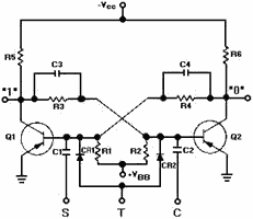
Figure 3-28. - Flip-flop with three inputs.
3-22
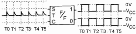
Figure 3-29. - Block diagram of a flip-flop with a toggle input.
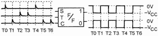
Figure 3-30. - Flip-flop with three inputs (block diagram).
Remember, a SET input will SET the flip-flop if it is in the CLEAR state, otherwise,
it will not do anything; a trigger at the CLEAR input can only CLEAR the circuit
if it is SET; and a trigger applied to the TOGGLE input will cause the bistable
multivibrator to change states regardless of what state it is in.
Q7. In a bistable multivibrator, how many trigger pulses are needed
to produce one complete cycle in the output?
Q8. How many stable states are there for a flip-flop?
Q9. If a voltage (positive or negative) is measured on the "1" output
of a flip-flop, what state is it in?
BlockING Oscillator
The BlockING Oscillator is a special type of wave generator used to produce a
narrow pulse, or trigger. Blocking oscillators have many uses, most of which are
concerned with the timing of some other circuit. They can be used as frequency dividers
or counter circuits and for switching other circuits on and off at specific times.
In a blocking oscillator the pulse width (pw), pulse repetition time (PRT), and
pulse repetition rate (PRR) are all controlled by the size of certain capacitors
and resistors and by the operating characteristics of the transformer. The transformer
primary determines the duration and shape of the output. Because of their importance
in the circuit, transformer action and series RL circuits will be discussed briefly.
You may want to review transformer action in NEETS, Module 2, Introduction to Alternating
Current and Transformers before going to the next section.
Transformer Action
Figure 3-31, view (A), shows a transformer with resistance in both the primary
and secondary circuits. If S1 is closed, current will flow through R1 and L1. As
the current increases in L1, it induces a voltage into L2 and causes current flow
through R2. The voltage induced into L2 depends on the ratio of turns between L1
and L2 as well as the current flow through L1.
3-23
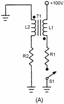
Figure 3-31A. - RL circuit.
The secondary load impedance, R2, affects the primary impedance through
reflection from secondary to primary. If the load on the secondary is increased
(R2 decreased), the load on the primary is also increased and primary and secondary
currents are increased.
T1 can be shown as an inductor and R1-R2 as a combined or equivalent series resistance
(RE) since T1 has an effective inductance and any change in R1 or R2
will change the current. The equivalent circuit is shown in figure 3-31, view (B).
It acts as a series RL circuit and will be discussed in those terms.
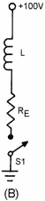
Figure 3-31B. - RL circuit.
3-24
Simple Series RL Circuit
When S1 is closed in the series RL circuit (view (B) of figure 3-31) L acts as
an open at the first instant as source voltage appears across it. As current begins
to flow, EL decreases and ER and I increase, all at exponential
rates. Figure 3-32, view (A), shows these exponential curves. In a time equal to
5 time constants the resistor voltage and current are maximum and EL
is zero. This relationship is shown in the following formula:

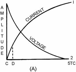
Figure 3-32A. - Voltage across a coil.
If S1 is closed, as shown in figure 3-31, view (B), the current will follow curve
1 as shown in figure 3-32, view (A). The time required for the current to reach
maximum depends on the size of L and RE. If RE is small, then the
RL circuit has a long time constant. If only a small portion of curve 1 (C to D
of view (A)) is used, then the current increase will have maximum change in a given
time period. Further, the smaller the time increment the more nearly linear is the
current rise. a constant current increase through the coil is a key factor in a
blocking oscillator.
Blocking Oscillator Applications
A basic principle of inductance is that if the increase of current through a
coil is linear; that is, the rate of current increase is constant with respect to
time, then the induced voltage will be constant. This is true in both the primary
and secondary of a transformer. Figure 3-32, view (B), shows the voltage waveform
across the coil when the current through it increases at a constant rate. Notice
that this waveform is similar in shape to the trigger pulse shown earlier in figure
3-1, view (E). By definition, a blocking oscillator is a special type of oscillator
which uses inductive regenerative feedback. The output
3-25
duration and frequency of such pulses are determined by the characteristics of
a transformer and its relationship to the circuit. Figure 3-33 shows a blocking
oscillator. This is a simplified form used to illustrate circuit operation.
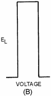
Figure 3-32B. - Voltage across a coil.
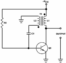
Figure 3-33. - Blocking oscillator.
When power is applied to the circuit, R1 provides forward bias and transistor
Q1 conducts. Current flow through Q1 and the primary of T1 induces a voltage in
L2. The phasing dots on the transformer indicate a 180-degree phase shift. As the
bottom side of L1 is going negative, the bottom side of L2 is going positive. The
positive voltage of L2 is coupled to the base of the transistor through C1, and
Q1 conducts more. This provides more collector current and more current through
L1. This action is regenerative feedback. Very rapidly, sufficient voltage is applied
to saturate the base of Q1. Once the base becomes saturated, it loses control over
collector current. The circuit now can be compared to a small resistor (Q1) in series
with a relatively large inductor (L1), or a series RL circuit.
3-26
The operation of the circuit to this point has generated a very steep leading
edge for the output pulse. Figure 3-34 shows the idealized collector and base waveforms.
Once the base of Q1 (figure 3-33) becomes saturated, the current increase in L1
is determined by the time constant of L1 and the total series resistance. From T0
to T1 in figure 3-34 the current increase (not shown) is approximately linear. The
voltage across L1 will be a constant value as long as the current increase through
L1 is linear.
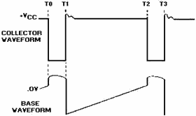
Figure 3-34. - Blocking oscillator idealized waveforms.
At time T1, L1 saturates. At this time, there is no further change in magnetic
flux and no coupling from L1 to L2. C1, which has charged during time to to T1,
will now discharge through R1 and cut off Q1. This causes collector current to stop,
and the voltage across L1 returns to 0.
The length of time between T0 and T1 (and T2 to T3 in the next cycle) is the
pulse width, which depends mainly on the characteristics of the transformer and
the point at which the transformer saturates. a transformer is chosen that will
saturate at about 10 percent of the total circuit current. This ensures that the
current increase is nearly linear. The transformer controls the pulse width because
it controls the slope of collector current increase between points T0 and T1. Since
TC = L ÷ R , the greater the L, the longer the TC. The longer the time constant,
the slower the rate of current increase. When the rate of current increase is slow,
the voltage across L1 is constant for a longer time. This primarily determines the
pulse width.
From T1 to T2 (figure 3-34), transistor Q1 is held at cutoff by C1 discharging
through R1 (figure
3-33). The transistor is now said to be "blocked." As C1 gradually loses its
charge, the voltage on the base of Q1 returns to a forward-bias condition. At T2,
the voltage on the base has become sufficiently positive to forward bias Q1, and
the cycle is repeated.
The collector waveform may have an INDUCTIVE OVERSHOOT (PARASITIC OSCILLATIONS)
at the end of the pulse. When Q1 cuts off, current through L1 ceases, and the magnetic
field collapses, inducing a positive voltage at the collector of Q1. These oscillations
are not desirable, so some means must be employed to reduce them. The transformer
primary may be designed to have a high dc resistance resulting in a low Q; this
resistance will decrease the amplitude of the oscillations. However, more damping
may be necessary than such a low-Q transformer primary alone can achieve. If so,
a DAMPING resistor can be placed in parallel with L1, as shown in figure 3-35.
3-27
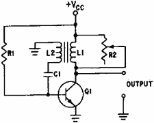
Figure 3-35. - Circuit damping.
When an external resistance is placed across a tank, the formula for the Q of
the tank circuit is Q = R/XL, where R is the equivalent total circuit
resistance in parallel with L. You should be able to see from the equation that
the Q is directly proportional to the damping resistance (R). In figure 3-35, damping
resistor R2 is used to adjust the Q which reduces the amplitude of overshoot parasitic
oscillations. As R2 is varied from infinity toward zero, the decreasing resistance
will load the transformer to the point that pulse amplitude, pulse width, and prf
are affected. If reduced enough, the oscillator will cease to function. By varying
R2, varying degrees of damping can be achieved, three of which are shown in figure
3-36, view (A), view (B and view (C).
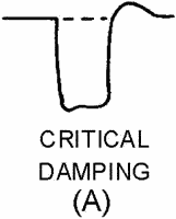
Figure 3-36A. - Waveform damping. CRITICAL DAMPING.
3-28
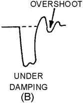
Figure 3-36B. - Waveform damping. UNDER DAMPING.
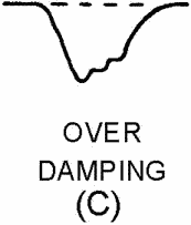
Figure 3-36C. - Waveform damping. OVER DAMPING.
CRITICAL DAMPING gives the most rapid transient response without overshoot. This
is accomplished by adjusting R2 to achieve a waveform as shown in figure 3-36, view
(A). The resistance of R2 depends upon the Q of the transformer. View (A) shows
that oscillations, including the overshoot, are damping out.
UNDERDAMPING gives rapid transient response with overshoot caused by high or
infinite resistance as shown in figure 3-36, view (B). OVERDAMPING is caused by
very low resistance and gives a slow transient response. It may reduce the pulse
amplitude as shown in figure 3-36, view (C).
3-29
The blocking oscillator discussed is a free-running circuit. For a fixed prf,
some means of stabilizing the frequency is needed. One method is to apply external
synchronization triggers (figure 3-37), view (A) and view (B). Coupling capacitor
C2 feeds input synchronization (sync) triggers to the base of Q1.
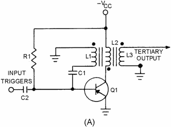
Figure 3-37A. - Blocking oscillator (synchronized).
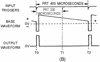
Figure 3-37B. - Blocking oscillator (synchronized).
If the trigger frequency is made slightly higher than the free-running
frequency, the blocking oscillator will "lock in" at the higher frequency. For instance,
assume the free-running frequency of this blocking oscillator is 2 kilohertz, with
a PRT of 500 microseconds. If sync pulses with a PRT of 400 microseconds, or 2.5
kilohertz, are applied to the base, the blocking oscillator will "lock in" and run
at 2.5 kilohertz. If the sync PRF is too high, however, frequency division will
occur. This means that if the sync
3-30
|