NEETS Module 9 − Introduction to Wave− Generation and Wave−Shaping
Pages i,
1−1,
1−11,
1−21,
1−31,
1−41,
2−1,
2−11,
2−21,
2−31,
3−1,
3−11,
3−21,
3−31,
3−41,
3−51,
4−1,
4−11,
4−21,
4−31,
4−41,
4−51, Index
| - |
Matter, Energy,
and Direct Current |
| - |
Alternating Current and Transformers |
| - |
Circuit Protection, Control, and Measurement |
| - |
Electrical Conductors, Wiring Techniques,
and Schematic Reading |
| - |
Generators and Motors |
| - |
Electronic Emission, Tubes, and Power Supplies |
| - |
Solid-State Devices and Power Supplies |
| - |
Amplifiers |
| - |
Wave-Generation and Wave-Shaping Circuits |
| - |
Wave Propagation, Transmission Lines, and
Antennas |
| - |
Microwave Principles |
| - |
Modulation Principles |
| - |
Introduction to Number Systems and Logic Circuits |
| - |
- Introduction to Microelectronics |
| - |
Principles of Synchros, Servos, and Gyros |
| - |
Introduction to Test Equipment |
| - |
Radio-Frequency Communications Principles |
| - |
Radar Principles |
| - |
The Technician's Handbook, Master Glossary |
| - |
Test Methods and Practices |
| - |
Introduction to Digital Computers |
| - |
Magnetic Recording |
| - |
Introduction to Fiber Optics |
| Note: Navy Electricity and Electronics Training
Series (NEETS) content is U.S. Navy property in the public domain. |
The schematic for a monostable multivibrator is
shown in figure 3-11. Like the astable multivibrator, one transistor conducts and
the other cuts off when the circuit is energized.
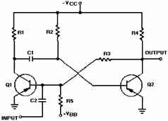
Figure 3-11. - Monostable multivibrator schematic.
Recall that when the astable multivibrator was first energized, it was impossible
to predict which transistor would initially go to cutoff because of circuit symmetry.
The one-shot circuit is not symmetrical like the astable multivibrator. Positive
voltage VBB is applied through R5 to the base of Q1. This positive voltage
causes Q1 to cut off. Transistor Q2 saturates because of the negative voltage applied
from -VCC to its base through R2. Therefore, Q1 is cut off and Q2 is
saturated before a trigger pulse is applied, as shown in figure 3-12. The circuit
is shown in its stable state.
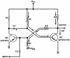
Figure 3-12. - Monostable multivibrator (stable state).
Let's take a more detailed look at the circuit conditions in this stable state
(refer to figure 3-12). As stated above, Q1 is cut off, so no current flows through
R1, and the collector of Q1 is at -VCC. Q2 is saturated and has practically
no voltage drop across it, so its collector is essentially at 0 volts. R5 and R3
form a voltage divider from VBB to the ground potential at the collector of
Q2. The tie point between these two resistors will be positive. Thus, the base of
Q1 is held positive, ensuring that Q1 remains cutoff. Q2
3-11
will remain saturated because the base of Q2 is very slightly negative as a result
of the voltage drop across R2. If the collector of Q1 is near -VCC
and the base of Q2 is near ground, C1 must be charged to nearly VCC
volts with the polarity shown.
Now that all the components and voltages have been described for the stable state,
let us see how the circuit operates (see figure 3-13). Assume that a negative pulse
is applied at the input terminal. C2 couples this voltage change to the base of
Q1 and starts Q1 conducting. Q1 quickly saturates, and its collector voltage immediately
rises to ground potential. This sharp voltage increase is coupled through C1 to
the base of Q2, causing Q2 to cut off; the collector voltage of Q2 immediately drops
to VCC. The voltage divider formed by R5 and R3 then holds the base of Q1 negative,
and Q1 is locked in saturation.
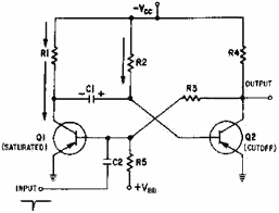
Figure 3-13. - Monostable multivibrator (triggered).
The one-shot multivibrator has now been turned on by applying a pulse at the
input. It will turn itself off after a period of time. To see how it does this,
look at figure 3-13 again. Q1 is held in saturation by the negative voltage applied
through R3 to its base, so the circuit cannot be turned off here. Notice that the
base of Q2 is connected to C1. The positive charge on C1 keeps Q2 cutoff. Remember
that a positive voltage change (essentially a pulse) was coupled from the collector
of Q1 when it began conducting to the base of Q2, placing Q2 in cutoff. When the
collector of Q1 switches from -VCC volts to 0 volts, the charge
on C1 acts like a battery with its negative terminal on the collector of Q1, and
its positive terminal connected to the base of Q2. This voltage is what cuts off
Q2. C1 will now begin to discharge through Q1 to ground, back through -VCC,
through R2 to the other side of C1. The time required for C1 to discharge depends
on the RC time constant of C1 and R2. Figure 3-14 is a timing diagram that shows
the negative input pulse and the resultant waveforms that you would expect to see
for this circuit description.
3-12
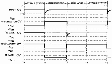
Figure 3-14. - Waveforms of a monostable multivibrator (triggered).
The only part of the operation not described so far is the short C1 charge time
that occurs right after Q1 and Q2 return to their stable states. This is simply
the time required for C1 to gain electrons on its left side. This charge time is
determined by the R1C1 time constant.
Another version of the monostable multivibrator is shown in figure 3-15. View
(A) is the circuit and view (B) shows the associated waveforms. In its stable condition
(T0), Q1 is cut off and Q2 is conducting. The input trigger (positive pulse at T1)
is applied to the collector of Q1 and coupled by C1 to the base of Q2 causing Q2
to be cut off. The collector voltage of Q2 then goes -VCC. The more negative
voltage at the collector of Q2 forward biases Q1 through R4. With the forward bias,
Q1 conducts, and the collector voltage of Q1 goes to about 0 volts. C1 now discharges
and keeps Q2 cut off. Q2 remains cut off until C1 discharges enough to allow Q2
to conduct again (T2). When Q2 conducts again, its collector voltage goes toward
0 volts and Q1 is cut off. The circuit returns to its quiescent state and has completed
a cycle. The circuit remains in this stable state until the next trigger arrives
(T3).
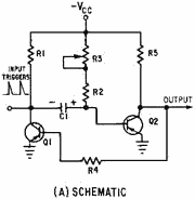
Figure 3-15A. - Monostable multivibrator and waveshapes. Schematic.
3-13
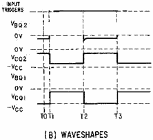
Figure 3-15B. - Monostable multivibrator and waveshapes. Waveshapes
Note that R3 is variable to allow adjustment of the gate width. Increasing R3
increases the discharge time for C1 which increases the cutoff time for Q2. Increasing
the value of R3 widens the gate. To decrease the gate width, decrease the value
of R3. Figure 3-16 shows the relationships between the trigger and the output signal.
View (A) of the figure shows the input trigger; views (B) and (C) show the different
gate widths made available by R3. Although the durations of the gates are different,
the duration of the complete cycle remains the same as the pulse repetition time
of the triggers. View (D) of the figure illustrates that the trailing edge of the
positive alternation is variable.
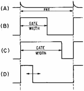
Figure 3-16. - Monostable multivibrator waveforms with a variable gate.
The reason the monostable multivibrator is also called a one-shot multivibrator
can easily be seen. For every trigger pulse applied to the multivibrator, a complete
cycle, or a positive and negative alternation of the output, is completed.
Q5. In an astable multivibrator, which components determine the pulse
repetition frequency?
3-14
Q6. What is another name for the monostable multivibrator?
Bistable Multivibrator
As the name implies, the bistable multivibrator has two stable states. If a trigger
of the correct polarity and amplitude is applied to the circuit, it will change
states and remain there until triggered again. The trigger need not have a fixed
PRF; in fact, triggers from different sources, occurring at different times, can
be used to switch this circuit.
The bistable multivibrator circuit and the associated waveforms are shown in
figure 3-17, views (A) and (B), respectively. In this circuit, R1 and R7 are the
collector load resistors. Voltage dividers R1, R2, and R5 provide forward bias for
Q2; R7, R6, and R3 provide forward bias for Q1. These resistors also couple the
collector signal from one transistor to the base of the other. Observe that this
is direct coupling of feedback. This type of coupling is required because the circuit
depends on input triggers for operation, not on RC time constants inside the circuit.
Both transistors use common emitter resistor R4 which provides emitter coupling.
C1 and C2 couple the input triggers to the transistor bases.
Figure 3-17A. - Bistable multivibrator and waveforms.
3-15
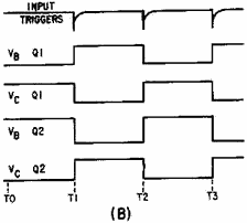
Figure 3-17B. - Bistable multivibrator and waveforms.
Notice that the circuit is symmetrical; that is, each transistor amplifier has
the same component values. When power is first applied, the voltage divider networks
place a negative voltage at the bases of Q1 and Q2. Both transistors have forward
bias and both conduct.
Due to some slight difference between the two circuits, one transistor will conduct
more than the other. Assume that Q1 conducts more than Q2. The increased conduction
of Q1 causes the collector voltage of Q1 to be less negative (more voltage drop
across R1). This decreases the forward bias of Q2 and decreases the conduction of
Q2. When Q2 conducts less, its collector voltage becomes more negative. The negative-going
change at the collector of Q2 is coupled to the base of Q1 and causes Q1 to conduct
even more heavily. This regenerative action continues until Q2 is cut off and Q1
is saturated. The circuit is in a stable state and will remain there until a trigger
is applied to change the state.
At T1, a negative trigger is applied to both bases through C1 and C2. The trigger
does not affect Q1 since it is already conducting. The trigger overcomes cutoff
bias on Q2 and causes it to conduct. As Q2 goes into conduction, its collector voltage
becomes positive. The positive-going change at the Q2 collector causes a reverse
bias on the base of Q1. As the conduction of Q1 decreases to the cutoff point, the
collector voltage becomes negative. This switching action causes a very rapid change
of state with Q2 now conducting and Q1 cut off.
At T2, a negative trigger is again applied to both bases. This time, Q1 is brought
into conduction and the regenerative switching action cuts off Q2. The bistable
multivibrator will continue to change states as long as triggers are applied. Notice
that two input triggers are required to produce one gate; one to turn it on and
the other to turn it off. The input trigger frequency is twice the output frequency.
The bistable multivibrator that most technicians know is commonly known by other
names: the ECCLES-JORDAN circuit and, more commonly, the FLIP-FLOP circuit (figure
3-18). The flip-flop is a bistable multivibrator, "bi" meaning two; that is, the
flip-flop has two stable states. The flip-flop (f/f) can rapidly flip from one state
to the other and then flop back to its original state. If a voltmeter were connected
to the output of a flip-flop, it would measure either a small positive or negative
voltage, or a particularly low voltage (essentially 0 volts). No matter which voltage
is measured, the flip-flop would be stable. Remember, stable means that the flip-flop
will remain in a particular state indefinitely. It will not change states unless
the proper type of trigger pulse is applied.
3-16
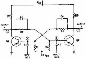
Figure 3-18. - Basic flip-flop.
Flip-flops are used in switching-circuit applications (computer logic operations)
as counters, shift registers, clock pulse generators, and in memory circuits. They
are also used for relay-control functions and for a variety of similar applications
in radar and communications systems.
Notice that the basic flip-flop, illustrated in figure 3-18, has two inputs and
two outputs. The inputs are coupled to the bases of the transistors and the outputs
are coupled from the collectors of the transistors. Think of the flip-flop as two
common-emitter amplifier circuits, where the output of one amplifier is connected
to the input of the other amplifier, and vice-versa. Point (D) is connected through
R4 to C4 to point (A). Point (A) is the input to transistor Q1. By the same token,
point (C), which is the output of Q1, is connected through R3 and C3 to the input
(point (B)) of transistor Q2.
Taking a close look at the flip-flop circuit, you should be able to see how it
maintains its stable condition. Typical values for the resistors and applied voltages
are shown in figure 3-19. The capacitors have been removed for simplicity.
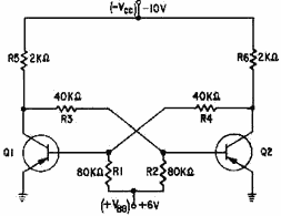
Figure 3-19. - Flip-flop (capacitors removed).
3-17
Two voltage-divider networks extend from -10 volts (V CC) to +6 volts (VBB).
One voltage divider consisting of resistors R1, R4, and R6 supplies the bias voltage
to the base of Q1. The other voltage divider consists of R2, R3, and R5 and supplies
the bias voltage to the base of Q2.
Assume that Q1 (figure 3-20) is initially saturated and Q2 is cut off. Recall
that the voltage drop from the base to the emitter of a saturated transistor is
essentially 0 volts. In effect, this places the base of Q1 at ground potential.
The voltages developed in the voltage divider, -VCC, R6, R4, R1, and
+VBB, are shown in the figure.
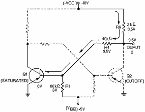
Figure 3-20. - Flip-flop (Q1 voltage divider).
Since no current flows through Q2, very little voltage is dropped across R6 (approximately
0.5 volt). The voltage at output 2 would measure -9.5 volts to ground (approximately
- VCC).
This voltage (-9.5 volts) is considered to be a High output. Figure 3-21 shows
the values of the other voltage-divider network.
3-18
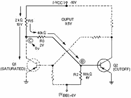
Figure 3-21. - Flip-flop (Q2 voltage divider).
With Q1 saturated, a large current flows through R5. The meter would measure
approximately 0 volts (ground potential) at point (C). Notice that point (B) is
located between point (C) (at 0 volts) and +VBB (at +6 volts).
The meter would measure a positive voltage (between 0 volts and +6 volts) at the
base of Q2 (point (B)).
a positive voltage on the base of a PNP transistor will cause that transistor
to cut off. If one transistor is saturated, the other must be cut off. The flip-flop
is stable in this state.
The capacitors that were removed from figure 3-19 must be returned to the flip-flop
as shown in figure 3-22 to change the state of the flip-flop from one condition
to the other. Capacitors C3 and C4 transmit almost instantaneously any changes in
voltage from the collector of one transistor to the base of the other. Capacitors
C1 and C2 are input coupling capacitors.
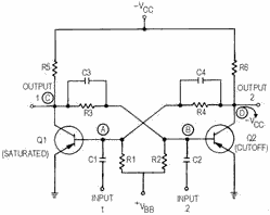
Figure 3-22. - Flip-flop.
3-19
As before, assume that transistor Q1 is saturated and transistor Q2 is cut off.
Two methods are available to cause the flip-flop to change states. First, a positive-going
pulse can be applied to input 1 to cause Q1 to change from saturation to cutoff.
Second, the same result can be achieved by applying a negative-going pulse to input
2. Transistor Q2 would then change from Cutoff to saturation. Normally, a pulse
is applied to the saturated transistor causing it to cut off. An input pulse which
is of the correct polarity to change the state of the flip-flop is, as before, called
a trigger pulse.
In figure 3-23 a positive-going trigger pulse has been applied to input 1. The
flip-flop has now changed states; Q1 is cut off and Q2 is saturated. If a second
positive-going trigger pulse is applied to input 1, it has no effect. This is because
Q1 is already cut off; therefore, a positive pulse on its base has no effect. But
if a positive-going trigger pulse were applied to input 2, the flip-flop would change
back to its original state as shown in figure 3-24.
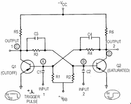
Figure 3-23. - Bistable multivibrator (flip-flop).
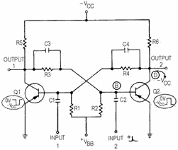
Figure 3-24. - Flip-flop (original state).
3-20
|