NEETS Module 9 − Introduction to Wave− Generation and Wave−Shaping
Pages i,
1−1,
1−11,
1−21,
1−31,
1−41,
2−1,
2−11,
2−21,
2−31,
3−1,
3−11,
3−21,
3−31,
3−41,
3−51,
4−1,
4−11,
4−21,
4−31,
4−41,
4−51, Index
| - |
Matter, Energy,
and Direct Current |
| - |
Alternating Current and Transformers |
| - |
Circuit Protection, Control, and Measurement |
| - |
Electrical Conductors, Wiring Techniques,
and Schematic Reading |
| - |
Generators and Motors |
| - |
Electronic Emission, Tubes, and Power Supplies |
| - |
Solid-State Devices and Power Supplies |
| - |
Amplifiers |
| - |
Wave-Generation and Wave-Shaping Circuits |
| - |
Wave Propagation, Transmission Lines, and
Antennas |
| - |
Microwave Principles |
| - |
Modulation Principles |
| - |
Introduction to Number Systems and Logic Circuits |
| - |
- Introduction to Microelectronics |
| - |
Principles of Synchros, Servos, and Gyros |
| - |
Introduction to Test Equipment |
| - |
Radio-Frequency Communications Principles |
| - |
Radar Principles |
| - |
The Technician's Handbook, Master Glossary |
| - |
Test Methods and Practices |
| - |
Introduction to Digital Computers |
| - |
Magnetic Recording |
| - |
Introduction to Fiber Optics |
| Note: Navy Electricity and Electronics Training
Series (NEETS) content is U.S. Navy property in the public domain. |
At T1 the +25 volts already across the capacitor and the +25 volts from the input
signal are in series and aid each other (Series AIDING). Thus, +50 volts appears
across R1 and D1. At this time, the cathode of D1 is positive with respect to the
anode, and the diode does not conduct. From T1 to T2, C1 discharges to approximately
+23 volts (because of the large values of R and C) and the output voltage drops
from +50 volts to +48 volts.
At T2 the input signal changes from +25 volts to -25 volts. The input is now
Series Opposing with the +23 volts across C1. This leaves an output voltage of -2
volts (-25 plus +23 volts). The cathode of D1 is negative with respect to the anode
and D1 conducts. From T2 to T3, C1 quickly charges through D1 from +23 volts to
+25 volts; the output voltage changes from -2 volts to 0 volts.
At T3 the input signal and capacitor voltage are again series aiding. Thus, the
output voltage felt across R1 and D1 is again +50 volts. During T3 and T4, C1 discharges
2 volts through R1. Notice that circuit operation from T3 to T4 is the same as it
was from T1 to T2. The circuit operation for each square- wave cycle repeats the
operation which occurred from T2 to T4.
Compare the input wave shape of figure 4-18, view (B), with the output wave shape.
Note the following important points: (1) The peak-to-peak amplitude of the input
wave shape has not been changed by the clamper circuit; (2) the shape of the output
wave shape has not been significantly changed from that of the input by the action
of the clamper circuit; and (3) the output wave shape is now all above 0 volts whereas
the input wave shape is both above and below 0 volts. Thus, the lower part of the
input
wave shape has been clamped to a dc potential of 0 volts in the output. This
circuit is referred to as a positive clamper since all of the output wave shape
is above 0 volts and the bottom is clamped at 0 volts.
The positive clamper circuit is self-adjusting. This means that the bottom of
the output waveform remains clamped at 0 volts during changes in input signal amplitude.
Also, the output wave shape retains the form and peak-to-peak amplitude (50 volts
in this case) of the input wave shape. When the input amplitude becomes greater,
the charge of the capacitor becomes greater and the output amplitude becomes larger.
When the input amplitude decreases, the capacitor does not charge as high as before
and clamping occurs at a lower output voltage. The capacitor charge, therefore,
changes with signal strength.
The size of R1 and C1 has a direct effect upon the operation of the clamper.
Because of the small resistance of the diode, the capacitor charge time is short.
If either R1 or C1 is made smaller, the capacitor discharges faster (TC = R · C).
The ability of a smaller value capacitor to quickly discharge to a lower voltage
is an advantage when the amplitude of the input wave shape is suddenly reduced.
However, for normal clamper operation, quick discharge time is a disadvantage. This
is because one objective of clamping is to keep the output wave shape the same as
the input wave shape. If the small capacitor allows a relatively large amount of
the voltage to discharge with each cycle, then distortion occurs in the output wave
shape. a larger portion of the wave shape then appears on the wrong side of the
reference line.
Increasing the value of the resistor increases the discharge time (again, TC
= R · C). This increased value causes the capacitor to discharge more slowly and
produces an output wave shape which is a better reproduction of the input wave shape.
a disadvantage of increasing the resistance value is that the larger resistance
increases the discharge time of the capacitor and slows the self-adjustment rate
of the circuit, particularly in case a sudden decrease in input amplitude should
occur. The larger resistance has no effect on self-adjustment with a sudden rise
in input amplitude. This is because the capacitor charges through the small resistance
of the conducting diode.
4-21
Circuits often incorporate a compromise between a short RC time constant (for
self-adjustment purposes) and a long RC time constant for less distortion. a point
to observe is that the reverse resistance of the diode sometimes replaces the, physical
resistor in the discharge path of the capacitor.
Positive-Diode Clamper With Bias
Biased clamping circuits operate in exactly the same manner as unbiased clampers,
with one exception. That exception is the addition of a dc bias voltage in series
with the diode and resistor. The size and polarity of this bias voltage determines
the output clamping reference.
View (A) of figure 4-19 illustrates the circuit of a positive clamper with positive
bias. It can be identified as a positive clamper because the cathode of the diode
is connected to the capacitor. Positive bias can be observed by noting that the
negative side of the battery is connected to ground. The purposes and actions of
the capacitor, resistor, and diode are the same as in the unbiased clamper circuit
just discussed.
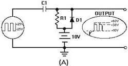
Figure 4-19A. - Positive clamper with positive bias.
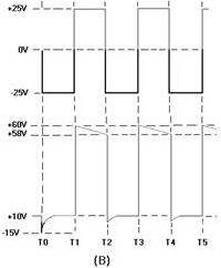
Figure 4-19B. - Positive clamper with positive bias.
4-22
With no input, D1 is forward biased and the +10 V battery is the output. C1 will
charge to +10 V and hold this charge until the first pulse is applied. The battery
establishes the dc reference level at +10 volts. The input wave shape at the top
of view (B) is a square wave which alternates between +25 and -25 volts. The output
wave shape is shown at the bottom half of view (B).
Here, as with previous circuits, let's apply Kirchhoff's voltage law to determine
circuit operation. With no input signal, the output is just the +10 volts supplied
by the battery.
At time T0 the -25 volt signal applied to the circuit is instantly felt across
R1 and D1. The -25 volt input signal forward biases D1, and C1 quickly charges to
35 volts. This leaves +10 volts across the output terminals for much of the period
from T0 to T1. The polarity of the charged capacitor is, from the left to the right,
minus to plus.
At T1 the 35 volts across the capacitor is series aiding with the +25 volt input
signal. At this point (T1) the output voltage becomes +60 volts; the voltage across
R1 and D1 is +50 volts, and the battery is +10 volts. The cathode of D1 is positive
with respect to the anode and the diode does not conduct. From T1 to T2, C1 discharges
only slightly through the large resistance of R1. Assume that, because of the size
of R1 and C1, the capacitor discharges just 2 volts (from +35 volts to +33 volts)
during this period. Thus, the output voltage drops from +60 volts to +58 volts.
At T2 the -25 volt input signal and the +33 volts across C1 are series opposing.
This makes the voltage across the output terminals +8 volts. The cathode of the
diode is 2 volts negative with respect to its anode and D1 conducts. Again, since
the forward-biased diode is essentially a short, C1 quickly charges from +33 volts
to +35 volts. During most of the time from T2 to T3, then, we find the output voltage
is +10 volts.
At T3 the +25 volts of the input signal is series aiding with the +35 volts across
C1. Again the output voltage is +60 volts. Observe that at T3 the conditions in
the circuit are the same as they were at T1. Therefore, the circuit operation from
T3 to T4 is the same as it was from T1 to T2. Circuit operation continues as a duplication
of the operations which occurred from T1 to T3.
By comparing the input and output wave shapes, you should note the following:
(1) The peak-to- peak amplitude of the input wave shape has not been changed in
the output (for all practical purposes) by the action of the clamper circuit; (2)
the shape of the input wave has not been changed; (3) the output wave shape is now
clamped above +10 volts. Remember that this clamping level (+10 volts) is determined
by the bias battery.
Positive-Diode Clamper With Negative Bias
View (A) of figure 4-20 is a positive clamper with negative bias. Observe that
with no input signal, the capacitor charges through R1 to the bias battery voltage;
the output voltage equals -10 volts. The circuit has negative bias because the positive
side of the battery is grounded. The output waveform is shown in view (B). Study
the figure and waveforms carefully and note the following important points. Once
again the peak-to-peak amplitude and shape of the output wave are, for all practical
purposes, the same as the input wave. The lower extremity of the output wave is
clamped to -10 volts, the value of the battery. Let's look at the circuit operation.
The capacitor is initially charged to -10 volts with no input signal, and diode
D1 does not conduct.
4-23
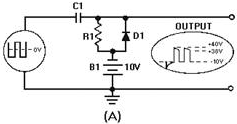
Figure 4-20A. - Positive clamper with negative bias.
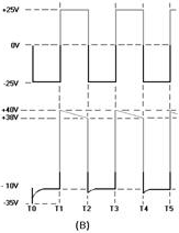
Figure 4-20B. - Positive clamper with negative bias.
The -25 volt input signal provides forward bias for D1. The capacitor charges
to +15 volts and retains most of its charge because its discharge through R1 is
negligible. The +25 volt input signal is series aiding the capacitor voltage and
develops +40 volts between the output terminals. When the input voltage is -25 volts,
D1 conducts and the output voltage is -10 volts (-25 volts plus +15 volts). In this
way the output reference is clamped at -10 volts. Changing the size of the battery
changes the clamping reference level to the new voltage.
Negative-DIODE CLAMPERS
Figure 4-21, view (A), illustrates the circuit of a negative-diode clamper. Compare
this with the positive-diode clamper in view (A) of figure 4-18. Note that the diode
is reversed with reference to ground. Like the positive clamper, resistor R1 provides
a discharge path for C1; the resistance must be a large value for C1 to have a long
discharge time. The low resistance of the diode provides a fast charge path for
C1. Once C1 becomes charged, it acts as a source of voltage which will help determine
the maximum and minimum voltage levels of the output wave shape. The input wave
shape shown in view (B) is a square wave which varies between +25 and -25 volts.
The output wave shapes are shown in the bottom half of view (B). You will find that
the operation of the negative clamper is similar to that of the positive clamper,
except for the reversal of polarities.
4-24
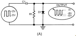
Figure 4-21A. - Negative clamper and waveform.
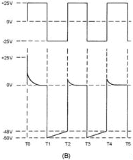
Figure 4-21B. - Negative clamper and waveform.
At T0 the +25 volt input signal applied to the circuit appears across R1 and
D1. This makes the anode of D1 positive with respect to the cathode and it conducts
heavily. Diode resistance is very small causing C1 to charge quickly. As the voltage
across C1 increases, the output voltage decreases. The voltage across C1 reaches
25 volts quickly; during most of T0 to T1, the output voltage is 0.
At T1 the voltage across the capacitor and the input voltage are series aiding
and result in -50 volts appearing at the output. At this time the diode is reverse
biased and does not conduct. Because of the size of R and C, the capacitor discharges
only 2 volts to approximately 23 volts from T1 to T2. Using Kirchhoff's voltage
law to determine voltage in the circuit, we find that the output voltage decreases
from -50 to -48 volts.
At T2 the +25 volt input signal and the 23 volts across C1 are series opposing.
The output voltage is +2 volts. The anode of D1 is positive with respect to the
cathode and D1 will conduct. From T2 to T3, C1 charges quickly from 23 to 25 volts
through D1. At the same time, the output voltage falls from +2 to 0 volts.
4-25
At T3 the input and capacitor voltages are series aiding and the total output
voltage is -50 volts. From T3 to T4, D1 is reverse biased and C discharges through
R. The circuit operation is now the same as it was from T1 to T2. The circuit operation
for the following square-wave cycles duplicates the operation which occurred from
T1 to T3.
As was the case with the positive clamper, the amplitude and wave, shape of the
output is almost identical to that of the input. However, note that the upper extremity
of the output wave shape is clamped to 0 volts; that is, the output wave shape,
for all practical purposes, lies entirely below the 0-volt reference level.
Negative-Diode Clamper With Negative Bias
View (A) of figure 4-22 is the circuit of a negative clamper with negative bias.
Again, with no input signal the capacitor charges to the battery voltage and the
output is negative because the positive side of the battery is ground. The bottom
of view (B) shows the output of the circuit. Study the figure carefully, and note
the following important points. The peak-to-peak amplitude and shape of the output
wave, for all practical purposes, are the same as that of the input wave. The output
wave is clamped to -10 volts which is the value of the battery. Since this is a
negative clamper, the upper extremity of the waveform touches the -10 volt reference
line (and the rest of it lies below this voltage level).
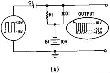
Figure 4-22A. - Negative damper with negative bias.
4-26
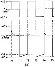
Figure 4-22B. - Negative damper with negative bias.
Let's review the important points of circuit operation. The capacitor is initially
charged to -10 volts with no input signal. Applying Kirchhoff's law we find that
the +25 volt input signal and the 10-volt battery are series opposing. This series
opposing forward biases D1 and the capacitor charges to -35 volts. The output voltage
is equal to the sum of the capacitor voltage and the input voltage. Thus, the output
voltage is -10 volts and the wave shape is clamped to -10 volts. With a -25 volt
input, the charge maintained across C1 and the input are series aiding and provide
a -60 volt output. C1 will discharge just before the next cycle begins and the input
becomes positive. The +25 volt input signal and the approximately -23 volt charge
remaining on C1 will forward bias D1 and the output will be clamped to the battery
voltage. C1 will quickly charge to the input signal level. Thus, the output voltage
varies between -10 and -60 volts and the wave shape is clamped to -10 volts.
Negative Clamper With Positive Bias
View (A) of figure 4-23 illustrates the circuit of a negative clamper with positive
bias. With no input signal the capacitor charges to the battery voltage and the
output is positive because the negative side of the battery is grounded. The output
is illustrated in the bottom half of view (B). Study the figure carefully and note
the following important points. The peak-to-peak amplitude and shape of the output
waveform, for all practical purposes, are the same as that of the input. The output
wave is clamped to +10 volts, the value of the battery. Since this is a negative
clamper (cathode to ground), the top of the output wave touches the +10 volt reference
line.
4-27
Figure 4-23A. - Negative clamper with positive bias.
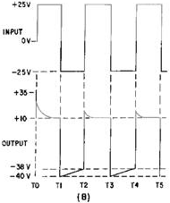
Figure 4-23B. - Negative clamper with positive bias.
Let's go over a summary of the circuit operation. With no input signal the capacitor
charges to 10 volts. The +25 volt input signal forward biases D1. With the 10-volt
battery and the input in series, the capacitor charges to -15 volts. The capacitor
remains charged, for all practical purposes, since its discharge through R1 (very
large) is almost negligible. The output voltage is equal to the algebraic sum of
the capacitor voltage and the input voltage. The +25 volt input signal added to
the -15 volt capacitor charge provides a +10 volt output. With a -25 volt input
at T1, D1 is reverse-biased and the charge across C 1 adds to the input voltage
to provide a -40 volt output. From T1 to T2, the capacitor loses only a small portion
of its charge. At T2 the input signal is +25 volts and the input returns to +10
volts. The wave shape is negatively clamped to +10 volts by the battery.
We can say, then, that positive clamping sets the wave shape above (negative
peak on) the reference level, and negative clamping places the wave shape below
(positive peak on) the reference level.
4-28
Q6. What is the relative length of the time constant for the diode-capacitor
combination in a damper (long or short)?
Q7. What is the relative length of the discharge time constant with
respect to the charge time constant of a damper (long or short)?
Q8. a positive damper clamps which extremity of the output signal
to 0 volts?
Q9. To which polarity does a positive damper with positive bins clamp
the most negative extremity of the output waveform (positive or negative)?
Q10. What type damper (with bias) clamps the most negative extremity
of the output waveform to a negative potential?
Q11. a negative damper damps which extremity of the output waveshape
to 0 volts?
Q12. a negative damper with negative bias clamps the most positive
extremity of the output wave shape to what polarity (positive or negative)?
Q13. What type of bias (positive or negative) is added to a negative
damper for the most positive extremity of the wave shape to be clamped above 0 volts?
Q14. What would be the output of a negative clamper with a bias potential
of -5 volts and an input voltage swing from +50 to -50 volts?
Common-Base Transistor CLAMPER
The common-base transistor clamper is similar to the dual diode limiter in figure
4-15, except for the addition of a transistor. In the previous clampers, we have
clamped the output signal to a reference. In the transistor common-base clamper,
we want to clamp the amplitude of the input to no more than nor less than certain
values in the output. Also, we do not want phase inversion in the output. View (A)
of figure
4-24 shows such a circuit. The transistor does not amplify the input and the
output is not inverted. However, the two diode circuits serve to clamp the output
between -2 volts and -8 volts, no matter what the varying input positive and negative
extremes.
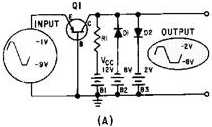
Figure 4-24A. - Common-base configuration clamper.
4-29
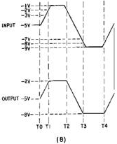
Figure 4-24B. - Common-base configuration clamper.
Look at view (B) as we continue. The input signal is a square-wave pulse type
signal that varies in amplitude. Without an input signal, Q1 conducts and provides
current through R1. This develops the output (collector to ground) potential which
is assumed to be approximately -5 volts (VCC - ER1)
for this discussion.
From T0 to T1 the output follows the input because of the increasing emitter-base
forward bias. However, at T1 the collector voltage reaches -2 volts and D2 is forward
biased. D2 conducts and limits the output to -2 volts (the value of B3). D2 conducts
until T2 when the input decreases below -2 volts. At this time, D2 cuts off and
the output again follows the input because of the decreasing forward bias on Q1.
At T3 the input reaches -8 volts and forward biases D1. D1 conducts and any further
increase (beyond -8 volts) of the input has no effect on the output. When the input
returns to a value more positive than -8 volts, D1 cuts off and the output again
follows the input. This circuit action is the same for all inputs. The output remains
the same as the input except that both positive and negative extremes are clamped
at -2 and -8 volts, respectively.
SHAPING Circuits
Timing circuits and circuits which require a particular shape or "spike" of voltage,
may use SHAPING circuits. Shaping circuits can be used to cause wave shapes, such
as square waves, sawtooth waves, and trapezoidal waves, to change their shape. Shaping
circuits may be either series RC or series RL circuits. The time constant is controlled
in respect to the duration of the applied waveform. Notice that the wave shapes
mentioned did not include the sine wave. These RC or RL shaping circuits do not
change the shape of a pure sine wave.
The series RC and RL circuits electrically perform the mathematical operations
of INTEGRATION and DIFFERENTIATION. Therefore, the circuits used to perform these
operations are called INTEGRATORS and DIFFERENTIATORS. These names are applied to
these circuits even though they do not always completely perform the operations
of mathematical integration and differentiation.
4-30
|