Module 7 - Introduction to Solid-State Devices and Power Supplies
|
||||||||||||||||||||||||||||||||||||||||||||||||||
|
Module 7 − Introduction to Solid−State Devices and Power Supplies
Pages i , 1−1, 1−11, 1−21, 1−31, 1−41, 2−1, 2−11, 2−21, 2−31, 2−41, 2−51, 3−1, 3−11, 3−21, 3−31, 3−41, 3−51, 4−1 to 4−10, 4−11, 4−21, 4−31, 4−41, 4−51, Index These NEETS training modules created by the U.S. Navy appear to have originally come out in 1990s and has been modernized a few times since then, so the information is fairly up to date. You will still find a lot of descriptions of vacuum tubes, but that is because even in 1998 the military still had a lot of legacy equipment that needed to be maintained. This particular module provides the student with an introduction to and history of semiconductor physics. The chapter runs a total of 62 pages so there's a lot of content. Chapter 1 - SEMICONDUCTOR DIODES Learning Objectives Learning objectives are stated at the beginning of each chapter. These learning objectives serve as a preview of the information you are expected to learn in the chapter. The comprehensive check questions are based on the objectives. By successfully completing the NRTC, you indicate that you have met the objectives and have learned the information. The learning objective are listed below. Upon completion of this chapter, you should be able to do the following: 1. State, in terms of energy bands, the differences between a conductor, an insulator, and a semiconductor. 2. Explain the electron and the hole flow theory in semiconductors and how the semiconductor is affected by doping. 3. Define the term "diode" and give a brief description of its construction and operation. 4. Explain how the diode can be used as a half-wave rectifier and as a switch. 5. Identify the diode by its symbology, alphanumerical designation, and color code. 6. List the precautions that must be taken when working with diodes and describe the different ways to test them. Introduction to SOLID-STATE DEVICES
Figure 1-1. - Size comparisons of electron tubes and semiconductors. As you recall from previous studies in this series, semiconductors have electrical properties somewhere between those of insulators and conductors. The use of semiconductor materials in electronic components is not new; some devices are as old as the electron tube. Two of the most widely known semiconductors in use today are the JUNCTION DIODE and Transistor. These semiconductors fall under a more general heading called solid-state devices. a SOLID-STATE DEVICE is nothing more than an electronic device, which operates by virtue of the movement of electrons within a solid piece of semiconductor material. Since the invention of the transistor, solid-state devices have been developed and improved at an unbelievable rate. Great strides have been made in the manufacturing techniques, and there is no foreseeable limit to the future of these devices. Solid-state devices made from semiconductor materials offer compactness, efficiency, ruggedness, and versatility. Consequently, these devices have invaded virtually every field of science and industry. In addition to the junction diode and transistor, a whole new family of related devices has been developed: the ZENER DIODE, LIGHT-EMITTING DIODE, FIELD EFFECT Transistor, etc. One development that has dominated solid-state technology, and probably has had a greater impact on the electronics industry than either the electron tube or transistor, is the INTEGRATED Circuit. The integrated circuit is a minute piece of semiconductor material that can produce complete electronic circuit functions.
As the applications of solid-state devices mount, the need for knowledge of these devices becomes increasingly important. Personnel in the Navy today will have to understand solid-state devices if they are to become proficient in the repair and maintenance of electronic equipment. Therefore, our objective in this module is to provide a broad coverage of solid-state devices and, as a broad application, power supplies. We will begin our discussion with some background information on the development of the semiconductor. We will then proceed to the semiconductor diode, the transistor, special devices and, finally, solid-state power supplies. SEMICONDUCTOR DEVELOPMENT Although the semiconductor was late in reaching its present development, its story began long before the electron tube. Historically, we can go as far back as 1883 when Michael Faraday discovered that silver sulfide, a semiconductor, has a negative temperature coefficient. The term negative temperature coefficient is just another way of saying its resistance to electrical current flow decreases as temperature increases. The opposite is true of the conductor. It has a positive temperature coefficient. Because of this particular characteristic, semiconductors are used extensively in power-measuring equipment. Only 2 years later, another valuable characteristic was reported by Munk A. Rosenshold. He found that certain materials have rectifying properties. Strange as it may seem, his finding was given such little notice that it had to be rediscovered 39 years later by F. Braun. Toward the close of the 19th century, experimenters began to notice the peculiar characteristics of the chemical element SELENIUM. They discovered that in addition to its rectifying properties (the ability to convert ac into dc), selenium was also light sensitive-its resistance decreased with an increase in light intensity. This discovery eventually led to the invention of the photophone by Alexander Graham Bell. The photophone, which converted variations of light into sound, was a predecessor of the radio receiver; however, it wasn't until the actual birth of radio that selenium was used to any extent. Today, selenium is an important and widely used semiconductor. Many other materials were tried and tested for use in communications. SILICON was found to be the most stable of the materials tested while GALENA, a crystalline form of lead sulfide, was found the most sensitive for use in early radio receivers. By 1915, Carl Beredicks discovered that GERMANIUM, another metallic element, also had rectifying capabilities. Later, it became widely used in electronics for low-power, low-frequency applications. Although the semiconductor was known long before the electron tube was invented, the semiconductor devices of that time could not match the performance of the tube. Radio needed a device that could not only handle power and amplify but rectify and detect a signal as well. Since tubes could do all these things, whereas semiconductor devices of that day could not, the semiconductor soon lost out. It wasn't until the beginning of World War II that interest was renewed in the semiconductor. There was a dire need for a device that could work within the ultra-high frequencies of radar. Electron tubes had interelectrode capacitances that were too high to do the job. The point-contact semiconductor diode, on the other hand, had a very low internal capacitance. Consequently, it filled the bill; it could be designed to work within the ultra-high frequencies used in radar, whereas the electron tube could not. As radar took on greater importance and communication-electronic equipment became more sophisticated, the demands for better solid-state devices mounted. The limitations of the electron tube made necessary a quest for something new and different. An amplifying device was needed that was smaller, lighter, more efficient, and capable of handling extremely high frequencies. This was asking a
lot, but if progress was to be made, these requirements had to be met. a serious study of semiconductor materials began in the early 1940's and has continued since. In June 1948, a significant breakthrough took place in semiconductor development. This was the discovery of Point-CONTACT Transistor. Here at last was a semiconductor that could amplify. This discovery brought the semiconductor back into competition with the electron tube. a year later, JUNCTION DIODES and Transistors were developed. The junction transistor was found superior to the point-contact type in many respects. By comparison, the junction transistor was more reliable, generated less noise, and had higher power-handling ability than its point-contact brother. The junction transistor became a rival of the electron tube in many uses previously uncontested. Semiconductor diodes were not to be slighted. The initial work of Dr. Carl Zener led to the development of ZENER DIODE, which is frequently used today to regulate power supply voltages at precise levels. Considerably more interest in the solid-state diode was generated when Dr. Leo Esaki, a Japanese scientist, fabricated a diode that could amplify. The device, named the TUNNEL DIODE, has amazing gain and fast switching capabilities. Although it is used in the conventional amplifying and oscillating circuits, its primary use is in computer logic circuits. Another breakthrough came in the late 1950's when it was discovered that semiconductor materials could be combined and treated so that they functioned as an entire circuit or subassembly rather than as a circuit component. Many names have been given to this solid-circuit concept, such as INTEGRATED Circuits, MICROELECTRONICS, and MICROCircuitRY. So as we see, in looking back, that the semiconductor is not something new, but it has come a long way in a short time. Q1. What is a solid-state device? Q2. Define the term negative temperature coefficient.
SEMICONDUCTOR Applications In the previous paragraphs, we mentioned just a few of the many different applications of semiconductor devices. The use of these devices has become so widespread that it would be impossible to list all their different applications. Instead, a broad coverage of their specific application is presented. Semiconductor devices are all around us. They can be found in just about every commercial product we touch, from the family car to the pocket calculator. Semiconductor devices are contained in television sets, portable radios, stereo equipment, and much more. Science and industry also rely heavily on semiconductor devices. Research laboratories use these devices in all sorts of electronic instruments to perform tests, measurements, and numerous other experimental tasks. Industrial control systems (such as those used to manufacture automobiles) and automatic telephone exchanges also use semiconductors. Even today heavy-duty versions of the solid- state rectifier diode are being use to convert large amounts of power for electric railroads. Of the many different applications for solid-state devices, space systems, computers, and data processing equipment are some of the largest consumers. The various types of modem military equipment are literally loaded with semiconductor devices. Many radars, communication, and airborne equipment are transistorized. Data display systems, data processing units, computers, and aircraft guidance-control assemblies are also good examples of
electronic equipments that use semiconductor devices. All of the specific applications of semiconductor devices would make a long impressive list. The fact is, semiconductors are being used extensively in commercial products, industry, and the military. SEMICONDUCTOR COMPETITION It should not be difficult to conclude, from what you already know, that semiconductor devices can and do perform all the conventional functions of rectification, amplification, oscillation, timing, switching, and sensing. Simply stated, these devices perform the same basic functions as the electron tube; but they perform more efficiently, economically, and for a longer period of time. Therefore, it should be no surprise to you to see these devices used in place of electron tubes. Keeping this in mind, we see that it is only natural and logical to compare semiconductor devices with electron tubes. Physically, semiconductor devices are much smaller than tubes. You can see in figure 1-1 that the difference is quite evident. This illustration shows some commonly used tube sizes alongside semiconductor devices of similar capabilities. The reduction in size can be as great as 100:1 by weight and 1000:1 by volume. It is easy to see that size reduction favors the semiconductor device. Therefore, whenever miniaturization is required or is convenient, transistors are favored over tubes. Bear in mind, however, that the extent of practical size reduction is a big factor; many things must be considered. Miniature electron tubes, for example, may be preferred in certain applications to transistors, thus keeping size reduction to a competitive area. Power is also a two-sided story. For low-power applications, where efficiency is a significant factor, semiconductors have a decided advantage. This is true mainly because semiconductor devices perform very well with an extremely small amount of power; in addition, they require no filaments or heaters as in the case of the electron tube. For example, a computer operating with over 4000 solid-state devices may require no more than 20 watts of power. However, the same number of tubes would require several kilowatts of power. For high-power applications, it is a different story - tubes have the upper hand. The high-power tube has no equivalent in any semiconductor device. This is because a tube can be designed to operate
with over a thousand volts applied to its plate whereas the maximum allowable voltage for a transistor is limited to about 200 volts (usually 50 volts or less). A tube can also handle thousands of watts of power. The maximum power output for transistor generally ranges from 30 milliwatts to slightly over 100 watts. When it comes to ruggedness and life expectancy, the tube is still in competition. Design and functional requirements usually dictate the choice of device. However, semiconductor devices are rugged and long-lived. They can be constructed to withstand extreme vibration and mechanical shock. They have been known to withstand impacts that would completely shatter an ordinary electron tube. Although some specially designed tubes render extensive service, the life expectancy of transistors is better than three to four times that of ordinary electronic tubes. There is no known failure mechanism (such as an open filament in a tube) to limit the semiconductor's life. However, semiconductor devices do have some limitations. They are usually affected more by temperature, humidity, and radiation than tubes are. Q3. Name three of the largest users of semiconductor devices. Q4. State one requirement of an electron tube, which does not exist for semiconductors, that makes the tube less efficient than the semiconductor.
SEMICONDUCTOR THEORY To understand why solid-state devices function as they do, we will have to examine closely the composition and nature of semiconductors. This entails theory that is fundamental to the study of solid- state devices. Rather than beginning with theory, let's first become reacquainted with some of the basic information you studied earlier concerning matter and energy (NEETS, Module 1). ATOMIC STRUCTURE The universe, as we know it today, is divided into two parts: matter and energy. Matter, which is our main concern at this time, is anything that occupies space and has weight. Rocks, water, air, automobiles, clothing, and even our own bodies are good examples of matter. From this, we can conclude that matter may be found in any one of three states: SOLIDS, LIQUIDS, and GASES. All matter is composed of either an element or combination of elements. As you know, an element is a substance that cannot be reduced to a simpler form by chemical means. Examples of elements with which you are in contact everyday are iron, gold, silver, copper, and oxygen. At present, there are over 100 known elements of which all matter is composed. As we work our way down the size scale, we come to the atom, the smallest particle into which an element can be broken down and still retain all its original properties. The atoms of one element, however, differ from the atoms of all other elements. Since there are over 100 known elements, there must be over 100 different atoms, or a different atom for each element. Now let us consider more than one element at a time. This brings us to the term "compound." a compound is a chemical combination of two or more elements. Water, table salt, ethyl alcohol, and ammonia are all examples of compounds. The smallest part of a compound, which has all the characteristics of the compound, is the molecule. Each molecule contains some of the atoms of each of the elements forming the compound. Consider sugar, for example. Sugar in general terms is matter, since it occupies space and has weight. It is also a compound because it consists of two or more elements. Take a lump of sugar and crush
it into small particles; each of the particles still retains its original identifying properties of sugar. The only thing that changed was the physical size of the sugar. If we continue this subdividing process by grinding the sugar into a fine power, the results are the same. Even dissolving sugar in water does not change its identifying properties, in spite of the fact that the particles of sugar are now too small to be seen even with a microscope. Eventually, we end up with a quantity of sugar that cannot be further divided without its ceasing to be sugar. This quantity is known as a molecule of sugar. If the molecule is further divided, it is found to consist of three simpler kinds of matter: carbon, hydrogen, and oxygen. These simpler forms are called elements. Therefore, since elements consist of atoms, then a molecule of sugar is made up of atoms of carbon, hydrogen, and oxygen. As we investigate the atom, we find that it is basically composed of electrons, protons, and neutrons. Furthermore, the electrons, protons, and neutrons of one element are identical to those of any other element. There are different kinds of elements because the number and the arrangement of electrons and protons are different for each element. The electron carries a small negative charge of electricity. The proton carries a positive charge of electricity equal and opposite to the charge of the electron. Scientists have measured the mass and size of the electron and proton, and they know how much charge each possesses. Both the electron and proton have the same quantity of charge, although the mass of the proton is approximately 1,827 times that of the electron. In some atoms there exists a neutral particle called a neutron. The neutron has a mass approximately equal to that of a proton, but it has no electrical charge.
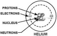
Figure 1-2. - The composition of a simple helium atom. According to theory, the electrons, protons, and neutrons of the atoms are thought to be arranged in a manner similar to a miniature solar system. Notice the helium atom in figure 1-2. Two protons and two neutrons form the heavy nucleus with a positive charge around which two very light electrons revolve. The path each electron takes around the nucleus is called an orbit. The electrons are continuously being acted upon in their orbits by the force of attraction of the nucleus. To maintain an orbit around the nucleus, the electrons travel at a speed that produces a counterforce equal to the attraction force of the nucleus. Just as energy is required to move a space vehicle away from the earth, energy is also required to move an electron away from the nucleus. Like a space vehicle, the electron is said to be at a higher energy level when it travels a larger orbit. Scientific experiments have shown that the electron requires a certain amount of energy to stay in orbit. This quantity is called the electron's energy level. By virtue of just its motion alone, the electron contains kinetic energy. Because of its position, it also contains potential energy. The total energy contained by an electron (kinetic energy plus potential energy) is the main factor that determines the radius of the electron's orbit. For an electron to remain in this orbit, it must neither gain nor lose energy.
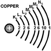
Figure 1-3. - Shell designation. The orbiting electrons do not follow random paths, instead they are confined to definite energy levels. Visualize these levels as shells with each successive shell being spaced a greater distance from the nucleus. The shells, and the number of electrons required to fill them, may be predicted by using Pauli's exclusion principle. Simply stated, this principle specifies that each shell will contain a maximum of 2n2 electrons, where n corresponds to the shell number starting with the one closest to the nucleus. By this principle, the second shell, for example, would contain 2(2) 2 or 8 electrons when full. In addition to being numbered, the shells are also given letter designations starting with the shell closest to the nucleus and progressing outward as shown in figure 1-3. The shells are considered to be full, or complete, when they contain the following quantities of electrons: 2 in the K(1st) shell, 8 in the L(2nd) shell, 18 in the M(3rd) shell, and so on, in accordance with the exclusion principle. Each of these shells is a major shell and can be divided into subshells, of which there are four, labeled s, p, d, and f. Like the major shells, the subshells are also limited as to the number of electrons they contain. Thus, the "s" subshell is complete when it contains 2 electrons, the "p" subshell when it contains 6, the "d" subshell when it contains 10, and the "f" subshell when it contains 14 electrons. Inasmuch as the K shell can contain no more than 2 electrons, it must have only one subshell, the s subshell. The M shell is composed of three subshells: s, p, and d. If the electrons in the s, p, and d subshells are added together, their total is found to be 18, the exact number required to fill the M shell. Notice the electron configuration of copper illustrated in figure 1-4. The copper atom contains 29 electrons, which completely fill the first three shells and subshells, leaving one electron in the "s" subshell of the N shell. a list of all the other known elements, with the number of electrons in each atom, is contained in the PERIODIC TABLE of ELEMENTS. The periodic table of elements is included in appendix 2.
Figure 1-4. - Copper atom. Valence is an atom's ability to combine with other atoms. The number of electrons in the outermost shell of an atom determines its valence. For this reason, the outer shell of an atom is called VALENCE SHELL, and the electrons contained in this shell are called VALENCE ELECTRONS. The valence of an atom determines its ability to gain or lose an electron, which in turn determines the chemical and electrical properties of the atom. An atom that is lacking only one or two electrons from its outer shell will easily gain electrons to complete its shell, but a large amount of energy is required to free any of its electrons. An atom having a relatively small number of electrons in its outer shell in comparison to the number of electrons required to fill the shell will easily lose these valence electrons. The valence shell always refers to the outermost shell. Q5. Define matter and list its three different states. Q6. What is the smallest particle into which an element can be broken down and still retain all its original properties? Q7. What are the three particles that comprise an atom and state the type of charge they hold? Q8. What is the outer shell of an atom called? ENERGY BandS Now that you have become reacquainted with matter and energy, we will continue our discussion with electron behavior. As stated earlier, orbiting electrons contain energy and are confined to definite energy levels. The various shells in an atom represent these levels. Therefore, to move an electron from a lower shell to a higher shell a certain amount of energy is required. This energy can be in the form of electric fields, heat, light, and even bombardment by other particles. Failure to provide enough energy to the electron, even if the energy supplied is just short of the required amount, will cause it to remain at its present energy level. Supplying more energy than is needed will only cause the electron to move to the next higher shell and the remaining energy will be wasted. In simple terms, energy is required in definite units to move electrons from one shell to the next higher shell. These units are called QUANTA (for example 1, 2, or 3 quanta).
Electrons can also lose energy as well as receive it. When an electron loses energy, it moves to a lower shell. The lost energy, in some cases, appears as heat. If a sufficient amount of energy is absorbed by an electron, it is possible for that electron to be completely removed from the influence of the atom. This is called IONIZATION. When an atom loses electrons or gains electrons in this process of electron exchange, it is said to be ionized. For ionization to take place, there must be a transfer of energy that results in a change in the internal energy of the atom. An atom having more than its normal amount of electrons acquires a negative charge, and is called a Negative ION. The atom that gives up some of its normal electrons is left with fewer negative charges than positive charges and is called a Positive ION. Thus, we can define ionization as the process by which an atom loses or gains electrons.
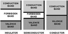
Figure 1-5. - The energy arrangement in atoms. Up to this point in our discussion, we have spoken only of isolated atoms. When atoms are spaced far enough apart, as in a gas, they have very little influence upon each other, and are very much like lone atoms. But atoms within a solid have a marked effect upon each other. The forces that bind these atoms together greatly modify the behavior of the other electrons. One consequence of this close proximity of atoms is to cause the individual energy levels of an atom to break up and form bands of energy. Discrete (separate and complete) energy levels still exist within these energy bands, but there are many more energy levels than there were with the isolated atom. In some cases, energy levels will have disappeared. Figure 1-5 shows the difference in the energy arrangement between an isolated atom and the atom in a solid. Notice that the isolated atom (such as in gas) has energy levels, whereas the atom in a solid has energy levels grouped into ENERGY BandS. The upper band in the solid lines in figure 1-5 is called the CONDUCTION Band because electrons in this band are easily removed by the application of external electric fields. Materials that have a large number of electrons in the conduction band act as good conductors of electricity. Below the conduction band is the forBIDDEN Band or energy gap. Electrons are never found in this band, but may travel back and forth through it, provided they do not come to rest in the band. The last band or VALENCE Band is composed of a series of energy levels containing valence electrons. Electrons in this band are more tightly bound to the individual atom than the electrons in the conduction band. However, the electrons in the valence band can still be moved to the conduction band with the application of energy, usually thermal energy. There are more bands below the valence band, but they are not important to the understanding of semiconductor theory and will not be discussed.
Figure 1-6. - Energy level diagram. The concept of energy bands is particularly important in classifying materials as conductors, semiconductors, and insulators. An electron can exist in either of two energy bands, the conduction band or the valence band. All that is necessary to move an electron from the valence band to the conduction band so it can be used for electric current, is enough energy to carry the electron through the forbidden band. The width of the forbidden band or the separation between the conduction and valence bands determines whether a substance is an insulator, semiconductor, or conductor. Figure 1-6 uses energy level diagrams to show the difference between insulators, semiconductors, and conductors. The energy diagram for the insulator shows the insulator with a very wide energy gap. The wider this gap, the greater the amount of energy required to move the electron from the valence band to the conduction band. Therefore, an insulator requires a large amount of energy to obtain a small amount of current. The insulator "insulates" because of the wide forbidden band or energy gap. The semiconductor, on the other hand, has a smaller forbidden band and requires less energy to move an electron from the valence band to the conduction band. Therefore, for a certain amount of applied voltage, more current will flow in the semiconductor than in the insulator. The last energy level diagram in figure 1-6 is that of a conductor. Notice, there is no forbidden band or energy gap and the valence and conduction bands overlap. With no energy gap, it takes a small amount of energy to move electrons into the conduction band; consequently, conductors pass electrons very easily. Q9. What term is used to describe the definite discrete amounts of energy required to move an electron from a low shell to a higher shell? Q10. What is a negative ion? Q11. What is the main difference in the energy arrangement between an isolated atom and the atom in a solid? Q12. What determines, in terms of energy bands, whether a substance is a good insulator, semiconductor, or conductor? COVALENT BONDING The chemical activity of an atom is determined by the number of electrons in its valence shell. When the valence shell is complete, the atom is stable and shows little tendency to combine with other atoms to form solids. Only atoms that possess eight valence electrons have a complete outer shell. These atoms are
1-10 <next>
|
||||||||||||||||||||||||||||||||||||||||||||||||||