Module 8 - Introduction to Amplifiers
Pages i,
1-1,
1-11,
1-21,
1-31,
2-1,
2-11,
2-21,
2-31,
3-1,
3-11,
3-21,
3-31,
3-41,
3-51,
3-61,
AI-1,
Index
| - |
Matter, Energy,
and Direct Current |
| - |
Alternating Current and Transformers |
| - |
Circuit Protection, Control, and Measurement |
| - |
Electrical Conductors, Wiring Techniques,
and Schematic Reading |
| - |
Generators and Motors |
| - |
Electronic Emission, Tubes, and Power Supplies |
| - |
Solid-State Devices and Power Supplies |
| - |
Amplifiers |
| - |
Wave-Generation and Wave-Shaping Circuits |
| - |
Wave Propagation, Transmission Lines, and
Antennas |
| - |
Microwave Principles |
| - |
Modulation Principles |
| - |
Introduction to Number Systems and Logic Circuits |
| - |
- Introduction to Microelectronics |
| - |
Principles of Synchros, Servos, and Gyros |
| - |
Introduction to Test Equipment |
| - |
Radio-Frequency Communications Principles |
| - |
Radar Principles |
| - |
The Technician's Handbook, Master Glossary |
| - |
Test Methods and Practices |
| - |
Introduction to Digital Computers |
| - |
Magnetic Recording |
| - |
Introduction to Fiber Optics |
| Note: Navy Electricity and Electronics Training
Series (NEETS) content is U.S. Navy property in the public domain. |
In addition to the other circuit components, an
amplifying device (transistor or electronic tube), itself, reacts differently to
high frequencies than it does to low frequencies. In earlier NEETS modules you were
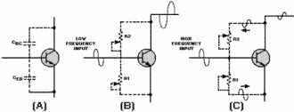
told that transistors and electronic tubes have interelectrode capacitance. Figure
2-5 shows a portion of the interelectrode capacitance of a transistor and the way
in which this affects high- and low-frequency signals.

Figure 2-5. - Interelectrode capacitance of a transistor.
In view (A) a transistor is shown with phantom capacitors connected to represent
the interelectrode capacitance. CEB represents the emitter-to-base capacitance.
CBC represents the base-to-collector capacitance.
For simplicity, in views (B) and (C) the capacitive reactance of these capacitors
is shown by variable resistors R1 (for CEB) and R2 (for CBC). View (B) shows the
reactance as high when there is a low-frequency input signal. In this case there
is very little effect from the reactance on the transistor. The transistor amplifies
the input signal as shown in view (B). However, when a high-frequency input signal
is applied to the transistor, as in view (C), things are somewhat different. Now
the capacitive reactance is low (as shown by the settings of the variable resistors).
In this case, as the base of the transistor attempts to go positive during the first
half of the input signal, a great deal of this positive signal is felt on the emitter
(through R1). If both the base and the emitter go positive at the same time, there
is no change in emitter-base bias and the conduction of the transistor will not
change. Of course, a small amount of change does occur in the emitter-base bias,
but not as much as when the capacitive reactance is higher (at low frequencies).
As an output signal is developed in the collector circuit, part of this signal is
fed back to the base through R2. Since the signal on the collector is 180 degrees
out of phase with the base signal, this tends to drive the base negative. The effect
of this is to further reduce the emitter-base bias and the conduction of the transistor.
During the second half of the input signal, the same effect occurs although the
polarity is reversed. The net effect is a reduction in the gain of the transistor
as indicated by the small output signal. This decrease in the amplifier output at
higher frequencies is caused by the interelectrode capacitance. (There are certain
special cases in which the feedback signal caused by the interelectrode capacitance
is in phase with the base signal. However, in most cases, the feedback caused by
interelectrode capacitance is degenerative and is 180 degrees out of phase with
the base signal as explained above.)
Q-4. What are the factors that limit the frequency response
of a transistor amplifier?
2-11
Q-5. What type of feedback is usually caused by interelectrode
capacitance?
Q-6. What happens to capacitive reactance as frequency increases?
Q-7. What happens to inductive reactance as frequency increases?
Video Amplifiers
As you have seen, a transistor amplifier is limited in its frequency response.
You should also remember from chapter 1 that a Video Amplifier should have a frequency
response of 10 hertz (10Hz) to 6 megahertz (6 MHz). The question has probably occurred
to you: How is it possible to "extend" the range of frequency response of an amplifier?
High-Frequency Compensation for Video Amplifiers
If the frequency-response range of an audio amplifier must be extended to 6 megahertz
(6 MHz) for use as a video amplifier, some means must be found to overcome the limitations
of the audio amplifier. As you have seen, the capacitance of an amplifier circuit
and the interelectrode capacitance of the transistor (or electronic tube) cause
the higher frequency response to be limited.
In some ways capacitance and inductance can be thought of as opposites. As stated
before, as frequency increases, capacitive reactance decreases, and inductive reactance
increases. Capacitance opposes changes in voltage, and inductance opposes changes
in current. Capacitance causes current to lead voltage, and inductance causes voltage
to lead current.
Since frequency affects capacitive reactance and inductive reactance in opposite
ways, and since it is the capacitive reactance that causes the problem with high-frequency
response, inductors are added to an amplifier circuit to improve the high-frequency
response. This is called High-Frequency Compensation. Inductors (coils), when used
for high-frequency compensation, are called Peaking Coils. Peaking coils can be
added to a circuit so they are in series with the output signal path or in parallel
to the output signal path. Instead of only in series or parallel, a combination
of peaking coils in series and parallel with the output signal path can also be used for high-frequency compensation.
As in all electronic circuits, nothing comes free. The use of peaking coils WILL
increase the frequency response of an amplifier circuit, but it will ALSO lower
the gain of the amplifier.
Series Peaking
The use of a peaking coil in series with the output signal path is known as Series
Peaking. Figure 2-6 shows a transistor amplifier circuit with a series peaking coil.
In this figure, R1 is the input-signal-developing resistor. R2 is used for bias
and temperature stability of Q1. C1 is the bypass capacitor for R2. R3 is the load
resistor for Q1 and develops the output signal. C2 is the coupling capacitor which
couples the output signal to the next stage. "Phantom" capacitor COUT represents
the output capacitance of the circuit, and "phantom" capacitor CIN represents
the input capacitance of the next stage.
2-12

Figure 2-6. - Series peaking coil.
You know that the capacitive reactance of COUT and CIN will limit
the high-frequency response of the circuit. L1 is the series peaking coil. It is
in series with the output-signal path and isolates COUT from CIN. R4 is called
a "swamping" resistor and is used to keep L1 from overcompensating at a narrow range
of frequencies. In other words, R4 is used to keep the frequency-response curve
flat. If R4 were not used with L1, there could be a "peak" in the frequency-response
curve. (Remember, L1 is called a peaking coil.)
Shunt Peaking
If a coil is placed in parallel (shunt) with the output signal path, the technique
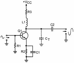
is called Shunt Peaking. Figure 2-7 shows a circuit with a shunt peaking coil. With
the exceptions of the "phantom" capacitor and the inductor, the components in this
circuit are the same as those in figure 2-6. R1 is the input-signal-developing resistor.
R2 is used for bias and temperature stability. C1 is the bypass capacitor for R2.
R3 is the load resistor for Q1 and develops the output signal. C2 is the coupling
capacitor which couples the output signal to the next stage.
2-13

Figure 2-7. - Shunt peaking coil.
The "phantom" capacitor, CT, represents the total capacitance of the circuit.
Notice that it tends to couple the output signal to ground.
L1 is the shunt peaking coil. While it is in series with the load resistor (R3),
it is in parallel (shunt) with the output-signal path.
Since inductive reactance increases as frequency increases, the reactance of
L1 develops more output signal as the frequency increases. At the same time, the
capacitive reactance of CT is decreasing as frequency increases. This tends
to couple more of the output signal to ground. The increased inductive reactance
counters the effect of the decreased capacitive reactance and this increases the
high-frequency response of the amplifier.
Combination Peaking
You have seen how a series peaking coil isolates the output capacitance of an
amplifier from the input capacitance of the next stage. You have also seen how a
shunt peaking coil will counteract the effects of the total capacitance of an amplifier.
If these two techniques are used together, the combination is more effective than
the use of either one alone. The use of both series and shunt peaking coils is known
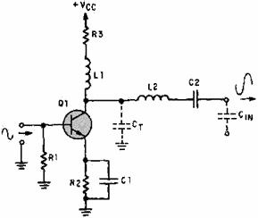
as Combination Peaking. An amplifier circuit with combination peaking is shown in
figure 2-8. In figure 2-8 the peaking coils are L1 and L2. L1 is a shunt peaking
coil, and L2 is a series peaking coil.
2-14

Figure 2-8. - Combination peaking.
The "phantom" capacitor CT represents the total capacitance of the amplifier
circuit. "Phantom" capacitor CIN represents the input capacitance of the next
stage. Combination peaking will easily allow an amplifier to have a high-frequency
response of 6 megahertz (6 MHz).
Q-8. What is the major factor that limits the high-frequency
response of an amplifier circuits?
Q-9. What components can be used to increase the high-frequency
response of an amplifier?
Q-10. What determines whether these components are considered
series or shunt?
Q-11. What is the arrangement of both series and shunt components
called?
Low-Frequency Compensation for Video Amplifiers
Now that you have seen how the high-frequency response of an amplifier can be
extended to 6 megahertz (6 MHz), you should realize that it is only necessary to
extend the low-frequency response to 10 hertz (10 Hz) in order to have a video amplifier.
Once again, the culprit in low-frequency response is capacitance (or capacitive
reactance). But this time the problem is the coupling capacitor between the stages.
At low frequencies the capacitive reactance of the coupling capacitor (C2 in
figure 2-8) is high. This high reactance limits the amount of output signal that
is coupled to the next stage. In addition, the RC network of the coupling capacitor
and the signal-developing resistor of the next stage cause a phase shift in the
output signal. (Refer to NEETS, Module 2, for a discussion of phase shifts in RC
networks.) Both of these problems (poor low-frequency response and phase shift)
can be solved by adding a parallel RC network in series with the load resistor.
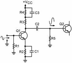
This is shown in figure 2-9.
2-15

Figure 2-9. - Low frequency compensation network.
The complete circuitry for Q2 is not shown in this figure, as the main concern
is the signal-developing resistor (R5) for Q2. The coupling capacitor (C2) and the
resistor (R5) limit the low-frequency response of the amplifier and cause a phase
shift. The amount of the phase shift will depend upon the amount of resistance and
capacitance. The RC network of R4 and C3 compensates for the effects of C2 and R5
and extends the low-frequency response of the amplifier.
At low frequencies, R4 adds to the load resistance (R3) and increases the gain
of the amplifier. As frequency increases, the reactance of C3 decreases. C3 then
provides a path around R4 and the gain of the transistor decreases. At the same
time, the reactance of the coupling capacitor (C2) decreases and more signal is
coupled to Q2.
Because the circuit shown in figure 2-9 has no high-frequency compensation, it
would not be a very practical video amplifier.
Typical Video-Amplifier Circuit
There are many different ways in which video amplifiers can be built. The particular
configuration of a video amplifier depends upon the equipment in which the video
amplifier is used. The circuit shown in figure 2-10 is only one of many possible
video-amplifier circuits. Rather than reading about what each component does in
this circuit, you can see how well you have learned about video amplifiers by answering
the following questions. You should have no problem identifying the purpose of the
components because similar circuits have been explained to you earlier in the text.
2-16

Figure 2-10. - Video amplifier circuit.
The following questions refer to figure 2-10.
Q-12. What component in an amplifier circuit tends to limit
the low-frequency response of the amplifier?
Q-13. What is the purpose of L3?
Q-14. What is the purpose of C1?
Q-15. What is the purpose of R4?
Q-16. What is the purpose of L2?
Q-17. What is the purpose of R5?
Q-18. What component(s) is/are used for high-frequency compensation
for Q1?
Q-19. What component(s) is/are used for low-frequency compensation
for Q2?
Radio-Frequency Amplifiers
Now that you have seen the way in which a broadband, or video, amplifier can
be constructed, you may be wondering about radio-frequency (RF) amplifiers. Do they use the same techniques? Are they just another type of broadband amplifier?
The answer to both questions is "no." Radio-frequency amplifiers use different
techniques than video amplifiers and are very different from them.
2-17
Before you study the specific techniques used in RF amplifiers, you should review
some information on the relationship between the input and output impedance of an
amplifier and the gain of the amplifier stage.
Amplifier Input/Output Impedance and Gain
You should remember that the gain of a stage is calculated by using the input
and output signals. The formula used to calculate the gain of a stage is:

Voltage gain is calculated using input and output voltage; current gain uses
input and output current; and power gain uses input and output power. For the purposes
of our discussion, we will only be concerned with voltage gain.
Figure 2-11 shows a simple amplifier circuit with the input- and output-signal-developing
impedances represented by variable resistors. In this circuit, C1 and C2 are the
input and output coupling capacitors. R1 represents the impedance of the input circuit.
R2 represents the input-signal-developing impedance, and R3 represents the output
impedance.

Figure 2-11. - Variable input and output impedances.
R1 and R2 form a voltage-divider network for the input signal. When R2 is increased
in value, the input signal to the transistor (Q1) increases. This causes a larger
output signal, and the gain of the stage increases.
Now look at the output resistor, R3. As R3 is increased in value, the output
signal increases. This also increases the gain of the stage.
As you can see, increasing the input-signal-developing impedance, the output
impedance, or both will increase the gain of the stage. Of course there are limits
to this process. The transistor must not be overdriven with too high an input signal
or distortion will result.
With this principle in mind, if you could design a circuit that had maximum impedance
at a specific frequency (or band of frequencies), that circuit could be used in
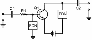
an RF amplifier. This Frequency- Determining Network could be used as the input-signal-developing
impedance, the output impedance, or both. The RF amplifier circuit would then be
as shown in figure 2-12.
2-18

Figure 2-12. - Semiblock diagram of RF amplifier.
In this "semi-block" diagram, C1 and C2 are the input and output coupling capacitors.
R1 represents the impedance of the input circuit. The blocks marked FDN represent
the frequency-determining networks. They are used as input-signal-developing and
output impedances for Q1.
Frequency-Determining Network for an RF Amplifier
What kind of circuit would act as a frequency-determining network? In general,
a frequency- determining network is a circuit that provides the desired response
at a particular frequency. This response could be maximum impedance or minimum impedance;
it all depends on how the frequency- determining network is used. You will see more
about frequency-determining networks in NEETS, Module 9 - Introduction to Wave-Generation
and Shaping Circuits. As you have seen, the frequency- determining network needed
for an RF amplifier should have maximum impedance at the desired frequency.
Before you are shown the actual components that make up the frequency-determining
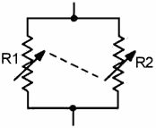
network for an RF amplifier, look at figure 2-13, which is a simple parallel circuit.
The resistors in this circuit are variable and are connected together (ganged) in
such a way that as the resistance of R1 increases, the resistance of R2 decreases,
and vice versa.

Figure 2-13. - Parallel variable resistors (ganged).
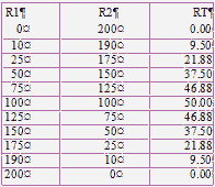
If each resistor has a range from 0 to 200 ohms, the following relationship will
exist between the individual resistances and the resistance of the network (RT).
(All values are in ohms, RT rounded off to two decimal places. These are selected
values; there are an infinite number of possible combinations.)
2-19

As you can see, this circuit has maximum resistance (RT) when the individual
resistors are of equal value. If the variable resistors represented impedances and
if components could be found that varied their impedance in the same way as the
ganged resistors in figure 2-13, you would have the frequency- determining network
needed for an RF amplifier.
There are components that will vary their impedance (reactance) like the ganged
resistors. As you know, the reactance of an inductor and a capacitor vary as frequency
changes. As frequency increases, inductive reactance increases, and capacitive reactance
decreases.
At some frequency, inductive and capacitive reactance will be equal. That frequency
will depend upon the value of the inductor and capacitor. If the inductor and capacitor
are connected as a parallel LC circuit, you will have the ideal frequency-determining
network for an RF amplifier.
The parallel LC circuit used as a frequency-determining network is called a Tuned
Circuit. This circuit is "tuned" to give the proper response at the desired frequency
by selecting the proper values of inductance and capacitance. a circuit using this
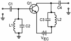
principle is shown in figure 2-14 which shows an RF amplifier with parallel LC circuits used as frequency-determining networks. This RF amplifier will only be effective
in amplifying the frequency determined by the parallel LC circuits.

Figure 2-14. - Simple RF amplifier.
In many electronic devices, such as radio or television receivers or radar systems,
a particular frequency must be selected from a band of frequencies. This could be
done by using a separate RF amplifier for each frequency and then turning on the
appropriate RF amplifier. It would be more efficient if a single RF amplifier could
be "tuned" to the particular frequency as that frequency is needed. This is what
2-20
|


