|
|||||||||||||
 |
|||||||||||||
Scattered Thoughts on Scattering Parameters |
|||||||||||||
|
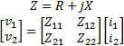
Sunshine Design Engineering Services See list of all of Joe's articles at bottom of page. Scattered Thoughts on Scattering Parameters By Joseph L. Cahak Copyright 2013 Sunshine Design Engineering Services Scattering parameters or S-parameters (aka Spars) are used by RF and microwave engineers to measure and design components and systems at those frequency ranges. These S-parameters are typically measured with an instrument called a vector network analyzer, or VNA. Complex Numbers and Parameters A complex number is represented by two values X and Y, as in X + iY = Z. X is the real component and iY is the imaginary component with Z being the complex representation. The letter ‘i' is used to designate the complex operator (√-1) by scientists and mathematicians, but in engineering the letter ‘j' is most often used. This is used to represent AC or RF signals. X may be the resistance and Y the reactance in ohms of the component to an AC signal. A standard RF load for instance is represented by 50 ohms real resistance and some reactance with good loads having reactance close to 0 ohms. X + iY can also represent a voltage and current as a function of time. Current is a function of the load and the voltage applied, so the resistances, voltages and currents are all important in describing a network for DC and AC (or RF) signals. A 2-port network can be represented by two equations with four parameters. The four parameters have different representations depending on what is known and what operations the users desire to use them for. Some network parameters (ABDC, S-, Z-, Y-, h-, etc.) are better than others depending on circuit types and the operations on them. Z Parameters Open circuit impedance parameters are used to represent the impedances of the network. The values are complex and represent real resistance (R) and reactance (jX) of the elements of the network.
Y Parameters Short circuit parameters or admittance parameters are used to represent the inverse of impedance. The real and imaginary parts are conductance (G) and susceptance (jB). The units are mhos or Siemens.
h Parameters Another model commonly used to analyze BJT (bipolar junction transistor) circuits is the h-parameter model, closely related to the hybrid-pi model and the y-parameter two-port model, but the h-parameter model uses input current and output voltage as independent variables, rather than input and output voltages. In this case it is a hybrid of an open circuit on the input and a short circuit on the output.
g Parameters Often this circuit is selected when a voltage amplifier is wanted at the output. The off-diagonal g-parameters are dimensionless, while diagonal members have dimensions the reciprocal of one another.
ABCD or T Parameters ABCD-parameters are known variously as chain, cascade, or transmission line parameters. This is useful for cascading 2 port network responses.
ABCD' or T' Parameters These are the inverse of the ABCD or T-parameters, respectively. They are useful for de-embedding 2-port network responses when multiplied with the ABCD matrix for the overall network.
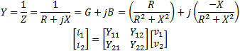
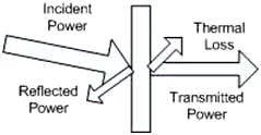
Network Transforms There are matrix transforms that are used to convert from one network description to another. Typically the S, Z, Y, h and ABCD are direct conversions. The conversion to a few of the others are after the base conversion and then converting from h to the inverse g for instance, ABCD with the inverse ABCD-1 and S-parameter to the T (one of the two types) or the anti-S parameter (S-1) . Note that the ABCD matrix is also known as a “T” matrix; this is not to be confused with the other two descriptions of a “T” matrix connected with the S-parameters calculations and will be presented in another paper. See Figure 1 for a graphical representation of the transformations available. Figure 1 - Network Description Transformations Transmission Lines Some of the transmission line functions and parameters are complex in value. They are excited by RF signals with most having complex modulation applied to them. Some basic measurement parameters need to be defined. A load can be represented at RF frequencies as a real resistance and an imaginary reactance driven by the charge delay or advancement as related to the driving voltage. This complex impedance is written as Z(ohms) = X + iY, with Z being complex value of the real (X) and imaginary (Y) components. Y is positive for an inductive element and negative for a capacitive element. Reflections When a RF signal is incident to a load, some of the signal is absorbed and converted to heat and radiated, what isn't absorbed is reflected back to the source as shown in Figure 2 and 3. Reflection coefficient represents this value in power measurements and is also known as rho or ρ = Γ = |Power Reflected/Power Incident|. Rho can be converted to the voltage standing wave ratio, or VSWR, by the equation VSWR = (1+ρ)/(1-ρ). These measurements are still scalar, but dimensionless. Rho and VSWR are measured in units of power (single dimension), but the ratio cancels the units out (thus dimensionless). Rho and VSWR can also be derived by the system impedances. The load can be represented by Z = R +jX. The measurement system used to characterize a component or another system also has impedance. This measurement with the device or network sets up an impedance match represented by gamma or Γ = (Zsys-Z)/(Zsys+Z) = (Power Reflected)/(Power Incident). The gamma, or complex reflection coefficient, can be transformed by absolute value to rho, or ρ=|Γ| , which can be used to derive the VSWR as given above. It can also be transformed by the system impedance to the load impedance.
Figure 2 – S11 or Gamma Source Signal Flow
Figure 3 - Power Reflected Transmission When a signal is incident to a 2-port network, the network looks like a load to the source, but the network has an output and a match at the output. The device has reflections from the output back to the input in addition to the transmitted part of the incident signal. As with the Reflection case, there is also some energy absorbed and converted to heat. The transmitted signal can be represented by Tau or τ = (Power Transmitted)/(Power Incident). See Figures 4 and 5.
Figure 4 - Transmission Network Signal Flow
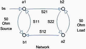
Figure 5 - Transmitted Power Units of Measurement Resistance is measured in ohms, voltage in volts, current in amps. Power is measured in watts. This can be referenced to a specific power level. Tradition and convention stipulate 1mW as 0 dBm. With this power can be represented in logarithmic units or decibels, dB for relative power gain or loss and dBm for absolute power level referenced to 1 mW. When power is measured the type of measurement makes a difference in how the units are converted. A Power Meter measures in Volt-Amps or true power as opposed to reactive or apparent power. The formula to convert real power to decibels is dB = 10*log10 [(Power Out)/(Power In)]. To convert measurements made in voltages, not true power, and this includes vector network analyzers, vector signal analyzers and spectrum Analyzers use the formula dB = 20*log10 [(Voltage Out)/(Voltage In)]. This can be derived from the fact that Power = Voltage2/Resistance , thus the doubling of the multiplier of the logarithm of the voltage ratio measurement of power. Convert dB to Watts using the inverse formulas: Watts = 10Power/10 and Watts=10Voltage20 . The absolute power can be converted between Watts and dBm with the following equations: Watts =10 (dBm/10) - 3 and dBm = 10*log10 (Watts*1000) dB units is a relative or ratio measurement. For power measurements adopted convention is to measure the signal relative to 1 mWatt for dBm and 1 V for dBV. S-Parameter Definitions S-parameters a and b components are in units of power represented as the square root of the power or Power Incident at Port 1 or a1 = V1+/√Zo Power Incident at Port 2 or a2 = V2+/√Zo Power Emitted at Port 1 or b1 = V1-/√Zo Power Emitted at Port 2 or b1 = V2-/√Zo b1 = S11a1 + S12a2 b2 = S21a1 + S22a2
Figure 6 - 2-Port S-Parameter Signal Flow Figure 6 shows the signal flow diagram for the S-Parameters. Note that the dimension of a1,a2 and b1,b2 are complex. These can then be used to derive the Scattering Parameters (Spars) for the network which are also complex values and dimensionless due to the ratio and in the case below are in rectangular coordinates and have linear magnitudes, not dB. Note that S-Parameters are dependent on the system Impedance. S-Parameters at one system impedance are not equal to S-Parameters at another System Impedance. S11 = b1/a1 or forward reflection coefficient S12 = b1/a2 or reverse transmission coefficient S21 = b2/a1 or forward transmission coefficient S22 = b2/a2 or reverse reflection coefficient Note also that the reflection coefficient for the load and source, ΓL = b2/a2 and Γs = b1/a1 , respectively are the same as S22 = b2/a2 and S11 = b1/a1 . In other words, if you measure the 1 port S-Parameter of a source or load, it is the same as the Gamma or Γ . These S-parameters are the basis of many RF and Microwave measurements. Network Analyzer Measurements In many RF and Microwave measurements the S-Parameters are typically expressed in dB (decibels) Magnitude units and Degrees in the polar coordinate system. Network and Vector Network Analyzers and Spectrum Analyzers all measure with voltage ratio measurements, so to convert to dB in terms of volts we must use the following equation. dB = 20*log10 [(Voltage Out)/(Voltage In)] Making measurements of S-parameters is a process of measurements made with calibrations standards (special components with values traceable to NIST or other designated agencies) and formulas to compute the correction factors from the measurement of those standards that determine a reference plane for the measurements. The measurement reference plane is an imaginary plane of reference for the measurements being made that lies somewhere between the measurement system's output and input ports, inclusive. It defines the points to which the network analyzer is calibrated to have 0 dB magnitude and 0 degrees phase response. It is the input and output planes to which reflection and transmission measurements are referenced. Another aspect of the relative measurement is that within the VNA dynamic range, the input power can be varied and the network response will stay the same until the power level goes outside the dynamic range. There are numerous methods and standards for coaxial, waveguide, planar, probe and other interconnections methods. There are also a number of test fixtures available and calibration techniques to help the test engineer make measurement in fixtures and give them the ability to de-embed fixture components to get at the raw device or subsystem S-parameters, which are difficult or nearly impossible to measure with standard equipment (e.g. mixed impedances). New Stuff I recently attended the Agilent “Back to Basics” seminar and as with the first one I attended 20 years ago, they still cover all the basics of measurements, S-parameters, measurement systems and how to use them. The new instruments all have the extended measurement capabilities built in with some really exciting capabilities. Spectrum analyzers can now reach down into the noise floor “Noise Floor Extension” and get to -172 dBm/Hz. This is a mere 2 dB from the theoretical noise limit at room temperature (recall that 25°C gives a 50 ohm noise power of -174 dBm in a 1 Hz bandwidth). The new oscilloscopes have some amazing features across the board and at lower costs. They have very high bit depth and are being used for the spectrum analyzer and vector signal analyzers (VSA) front ends, as they have in some cases more than 14 bits of ADC depth, thereby giving much greater dynamic range. Finally the exciting news on the vector network analyzer (VNA) measurement front is the new X-parameter test sets that can do large signal multi-harmonic, power and spurious analysis, in addition to the small signal S-parameters. This is important because now the non-linear characteristics of device and circuit response can be measured in addition to the linear characteristics. With this new information much more accurate device and circuit models can be formulated, yielding a more accurate model for designers to use in simulations. Conclusion We showed that S-parameters can be used for a number of network computations that can add value to measurements where the equipment is limited in features. The reader can find these equations and more in my S-Parameter Library (DLL & LLB) and my RF Calculator products. References www.AstroCalculator.com See RF Calculator and soon Labview S-Parameter Library https://en.wikipedia.org/wiki/Two-port_network https://en.wikipedia.org/wiki/S-parameters https://en.wikipedia.org/wiki/ABCD-parameters#ABCD-parameters https://en.wikipedia.org/wiki/Transmission_line https://en.wikipedia.org/wiki/Reflection_coefficient https://en.wikipedia.org/wiki/Standing_wave_ratio https://en.wikipedia.org/wiki/Electrical_impedance https://en.wikipedia.org/wiki/Admittance https://en.wikipedia.org/wiki/Two-port_network#Hybrid_parameters_.28h-parameters.29 https://en.wikipedia.org/wiki/X-parameters Making S-Parameter measurements in Mixed Impedances, Jim Hillstrom, Microwaves & RF, January 1992 Agilent PN 8720-2, In-fixture Microstrip Device Measurements Using TRL* Calibration, Product Note Agilent PN 8510-5A, Specifying Calibration Standards for the Agilent 8510 Agilent 8510-13, Measuring Noninsertable Devices, Product Note Agilent AN 1287-1, Understanding the Fundamental Principles of Vector Network Analysis, Application Note Agilent AN 1287-3, Applying Error Correction to Network Analyzer Measurements, Application Note Agilent Application Note 1287-7, Improving Network Analyzer Measurements of Frequency-translating Devices Agilent AN 1287-6, Using a Network Analyzer to Characterize High-Power Components, Application Note Agilent AN 1287-9, In-Fixture Measurements Using Vector Network Analyzers, Application Note Agilent AN 1364-1, De-embedding and Embedding S-Parameter Networks Using a Vector Network Analyzer Agilent DE-EMBEDDED MEASUREMENTS USING THE HP 8510 MICROWAVE NETWORK ANALYZER Agilent Network Analyzer Basics Agilent 5989-5765EN Agilent Signal Integrity Analysis Series Part 3: The ABCs of De-Embedding Application Note Agilent AN 154, S-Parameter Design, Application Note Agilent AN 95-1 S-Parameter Techniques for Faster more accurate Network Design Microwave Engineering, David M. Pozar, Wiley, ISBN 9971-51-263-7 Networks and Systems, D Roy Choudhury, Wiley, ISBN 0-470-20867-8 Fields and Waves in Communications Electronics, Ramo, Whinnery & Van Duzer, Wiley, ISBN Lib Congress Catalog 65-19477 High-Frequency Circuit Design and measurements, Peter Yip, Chapman and hall, 0-442-31185-0 Sunshine Design Engineering Services is located in the sunny San Vicente Valley near San Diego, CA, gateway to the mountains and skies. Are you looking for new things to design, program or create and need assistance? I offer design services with specialties in electronic hardware, CAD and software engineering, and 25 years of experience with Test Engineering services in RF/microwave, transceiver and semiconductor parametric test, test application program development, automation programs, database programming, graphics and analysis, and mathematical algorithms. See also: - Noise and Noise Measurements - Measuring Semiconductor Device Input Parameters with Vector Analysis - Computing with Scattering Parameters - Measurements with Scattering Parameters - Ponderings on Power Measurements - Scattered Thoughts on Scattering Parameters Sunshine Design Engineering Services 23517 Carmena Rd Ramona, CA 92065 760-685-1126 Featuring: Test Automation Services, RF Calculator and S-Parameter Library (DLL & LLB)
Posted August 1, 2013 |
|||||||||||||
 |
|||||||||||||
|
|||||||||||||


|
||||||||||||||||||||||||||||||||||||