|
|
|||||||||
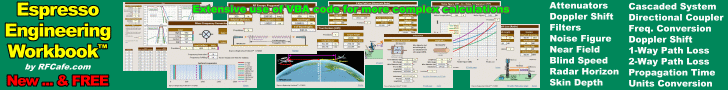
| Software: RF Cascade Workbook | RF Symbols for Office | RF Symbols & Stencils for Visio | Espresso Workbook | ||||||||||
|
|||||||||||||||||||||||||||||||
   |
   |
||||||||||||||||||||||||||||||
|
Please Support RF Cafe by purchasing my ridiculously low-priced products, all of which I created. RF & Electronics Symbols for Visio RF & Electronics Symbols for Office RF & Electronics Stencils for Visio T-Shirts, Mugs, Cups, Ball Caps, Mouse Pads These Are Available for Free |
|||||||||||||||||||||||||||||||


PCB Layer Stackup Calculator
San Francisco
Circuits


Press Release Archives:
Content is copyright of company represented. Page format, custom text and images are RF Cafe copyright - do not distribute. Note: Posting of press releases costs $100 each for non-advertisers.


San Francisco Circuits PCB Layer Stack-up Calculator
August 20, 2025 - San Mateo, California - San Francisco Circuits has launched a new PCB Stackup Calculator / Design Tool. San Francisco Circuits' free PCB Stackup Calculator helps engineers and designers quickly configure and visualize multilayer PCB stackups from 4 to 14 layers. Users can select copper weights, dielectric materials, and vias, then instantly view a detailed layer-by-layer breakdown with IPC 6012 manufacturing guidelines.
Key Benefits:
- Layer Flexibility - Design stackups for 4 to 14 layers
- Material Guidance - Typical copper foil and prepreg thicknesses
- Via Options - Blind and buried
- Instant Visualization - Clear stackup tables for easy review
Our engineering team can help optimize your stack-up and via strategy to meet stringent performance, size, and reliability requirements.
Read more including the full breakdown on the Types of PCB Vias on the San Francisco Circuits website.
About San Francisco Circuits
San Francisco Circuits is a provider of PCB fabrication and assembly, has a dedicated team specializing in simple and complex PCB fabrication and assembly technologies. They can produce elaborate and high-quality PCBs in a number of custom and common layouts. From basic to intricate PCBs–their engineers will meet your PCB fabrication & assembly needs. The company provides a rare balance between technical expertise and competitive pricing. And they not only provide high-quality products but also high-quality customer service at the same time. San Francisco Circuits has been voted by National Television as the "world's greatest in PCBs" and has demonstrated experience as a power player in PCB fabrication and assembly.
If you are looking to discuss PCB projects of any size or scope, feel free to reach out to them via our website (see below).
Contact
Victor Bilandzic
San Francisco Circuits, Inc.
Phone: 1-800-732-5143
Web: www.sfcircuits.com
Copyright: 1996 - 2026 |
About RF Cafe RF Cafe began life in 1996 as "RF Tools" in an AOL screen name web space totaling 2 MB. Its primary purpose was to provide me with ready access to commonly needed formulas and reference material while performing my work as an RF system and circuit design engineer. The World Wide Web (Internet) was largely an unknown entity at the time and bandwidth was a scarce commodity. Dial-up modems blazed along at 14.4 kbps while tying up your telephone line, and a lady's voice announced "You've Got Mail" when a new message arrived... |
Copyright 1996 - 2026 All trademarks, copyrights, patents, and other rights of ownership to images
and text used on the RF Cafe website are hereby acknowledge My Hobby Website: My Daughter's Website: |
