Module 12 − Modulation Principles
Pages i,
1−1,
1−11,
1−21,
1−31,
1−41,
1−51,
1−61,
1−71,
2−1,
2−11,
2−21,
2−31,
2−41,
2−51,
2−61,
3−1,
3−11,
3−21,
3−31, AI−1, Index, Assignment 1, 2
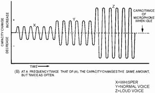
Figure 2-7B. - Capacitance change in an oscillator circuit during modulation. AT a Frequency TWICE THAT of (A), The
CAPACITY CHANGES The SAME AMOUNT, BUT TWICE AS ofTEN. Figure 2-8 shows how the frequency shift of an FM signal goes through the same variations as does the
modulating signal. In this figure the dimension of the constant amplitude is omitted. (As these remaining
waveforms are presented, be sure you take plenty of time to study and digest what the figures tell you. Look each
one over carefully, noting everything you can about them. Doing this will help you understand this material.) If
the maximum frequency deviation is set at 75 kilohertz above and below the carrier, the audio amplitude of the
modulating wave must be so adjusted that its peaks drive the frequency only between these limits. This can then be
referred to as 100-PERCENT MODULATION, although the term is only remotely applicable to fm. Projections along the
vertical axis represent deviations in frequency from the resting frequency (carrier) in terms of audio amplitude.
Projections along the horizontal axis represent time. The distance between a and B represents 0.001 second. This
means that carrier deviations from the resting frequency to plus 75 kilohertz, then to minus 75 kilohertz, and
finally back to rest would occur 1,000 times per second. This would equate to an audio frequency of 1,000 hertz.
Since the carrier deviation for this period (A to B) extends to the full allowable limits of plus and minus 75 kilohertz, the wave is fully modulated. The distance from C to D is the same as that from a to B, so the time
interval and frequency are the same as before. Notice, however, that the amplitude of the modulating wave has been
decreased so that the carrier is driven to only plus and minus 37.5 kilohertz, one-half the allowable deviation.
This would correspond to only 50-percent modulation if the system were AM instead of fm. Between E and F, the
interval is reduced to 0.0005 second. This indicates an increase in frequency of the modulating signal to 2,000
hertz. The amplitude has returned to its maximum allowable value, as indicated by the deviation of the carrier to
plus and minus 75 kilohertz. Interval G to H represents the same frequency at a lower modulation amplitude (66
percent). Notice the GUARD BandS between plus and minus 75 kilohertz and plus and minus 100 kilohertz. These bands
isolate the modulation extremes of this particular channel from that of adjacent channels. 2-11
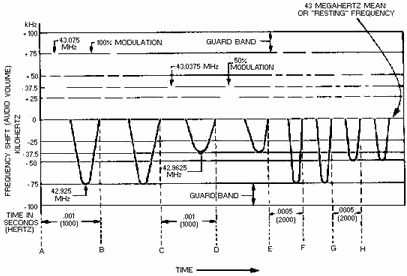
Figure 2-8. - Frequency-modulating signal. PERCENT of MODULATION. - Before we explain 100-percent modulation in an FM system, let's
review the conditions for 100-percent modulation of an AM wave. Recall that 100-percent modulation for AM exists
when the amplitude of the modulation envelope varies between 0 volts and twice its normal unmodulated value. At
100-percent modulation there is a power increase of 50 percent. Because the modulating wave is not constant in
voice signals, the degree of modulation constantly varies. In this case the vacuum tubes in an AM system cannot be
operated at maximum efficiency because of varying power requirements. In frequency modulation, 100-percent
modulation has a meaning different from that of AM. The modulating signal varies only the frequency of the
carrier. Therefore, tubes do not have varying power requirements and can be operated at maximum efficiency and the
FM signal has a constant power output. In FM a modulation of 100 percent simply means that the carrier is deviated
in frequency by the full permissible amount. For example, an 88.5-megahertz FM station operates at 100-percent
modulation when the modulating signal deviation frequency band is from 75 kilohertz above to 75 kilohertz below
the carrier (the maximum allowable limits). This maximum deviation frequency is set arbitrarily and will vary
according to the applications of a given FM transmitter. In the case given above, 50-percent modulation would mean
that the carrier was deviated 37.5 kilohertz above and below the resting frequency (50 percent of the
150-kilohertz band divided by 2). Other assignments for FM service may limit the allowable deviation to 50
kilohertz, or even 10 kilohertz. Since there is no fixed value for comparison, the term "percent of modulation"
has little meaning for fm. The term MODULATION Index is more useful in FM modulation discussions. Modulation index
is frequency deviation divided by the frequency of the modulating signal. 2-12
MODULATION Index. - This ratio of frequency deviation to frequency of the modulating
signal is useful because it also describes the ratio of amplitude to tone for the audio signal. These factors
determine the number and spacing of the side frequencies of the transmitted signal. The modulation index formula
is shown below:

Views (A) and (B) of figure 2-9 show the frequency spectrum for various FM signals. In the four examples of
view (A), the modulating frequency is constant; the deviation frequency is changed to show the effects of
modulation indexes of 0.5, 1.0, 5.0, and 10.0. In view (B) the deviation frequency is held constant and the
modulating frequency is varied to give the same modulation indexes.

Figure 2-9. - Frequency spectra of FM waves under various conditions. You can determine several facts about FM signals by studying the frequency spectrum. For example, table
2-1 was developed from the information in figure 2-9. Notice in the top spectrums of both views (A) and (B) that
the modulation index is 0.5. Also notice as you look at the next lower spectrums that the modulation index is 1.0.
Next down is 5.0, and finally, the bottom spectrums have modulation indexes of 2-13
10.0. This information was used to develop table 2-1 by listing the modulation indexes in the
left column and the number of significant sidebands in the right. SIGNIFICANT SIDEBandS (those with significantly
large amplitudes) are shown in both views of figure 2-9 as vertical lines on each side of the carrier frequency.
Actually, an infinite number of sidebands are produced, but only a small portion of them are of sufficient
amplitude to be important. For example, for a modulation index of 0.5 [top spectrums of both views (A) and (B)],
the number of significant sidebands counted is 4. For the next spectrums down, the modulation index is 1.0 and the
number of sidebands is 6, and so forth. This holds true for any combination of deviating and modulating
frequencies that yield identical modulating indexes.
Table 2-1. - Modulation index table

You should be able to see by studying figure 2-9, views (A) and (B), that the modulating frequency
determines the spacing of the sideband frequencies. By using a significant sidebands table (such as table 2-1),
you can determine the bandwidth of a given FM signal. Figure 2-10 illustrates the use of this table. The carrier
frequency shown is 500 kilohertz. The modulating frequency is 15 kilohertz and the deviation frequency is 75
kilohertz. 2-14
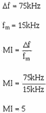

Figure 2-10. - Frequency deviation versus bandwidth. From table 2-1 we see that there are 16 significant sidebands for a modulation index of 5. To determine
total bandwidth for this case, we use:

The use of this math is to illustrate that the actual bandwidth of an FM transmitter (240 kHz) is
greater than that suggested by its maximum deviation bandwidth (±75 kHz or 150 kHz). This is important to know
when choosing operating frequencies or designing equipment. Q-4. What characteristic of a carrier wave
is varied in frequency modulation? Q-5. How is the degree of modulation expressed in an FM system?
Q-6. What two values may be used to determine the bandwidth of an FM wave? 2-15
Methods of Frequency MODULATION. - The circuit shown earlier in figure 2-6 and the
discussion in previous paragraphs were for illustrative purposes only. In reality, such a circuit would not be
practical. However, the basic principle involved (the change in reactance of an oscillator circuit in accordance
with the modulating voltage) constitutes one of the methods of developing a frequency- modulated wave. Reactance-Tube Modulation. - In direct modulation, an oscillator is frequency modulated by a REACTANCE TUBE that is
in parallel (Shunt) with the oscillator tank circuit. (The terms "shunt" or "shunting" will be used in this module
to mean the same as "parallel" or "to place in parallel with" components.) This is illustrated in figure 2-11. The
oscillator is a conventional Hartley circuit with the reactance-tube circuit in parallel with the tank circuit of
the oscillator tube. The reactance tube is an ordinary pentode. It is made to act either capacitively or
inductively; that is, its grid is excited with a voltage which either leads or lags the oscillator voltage by 90
degrees.

Figure 2-11. - Reactance-tube FM modulator.
When the reactance tube is connected across the tank circuit with no modulating voltage applied, it will
affect the frequency of the oscillator. The voltage across the oscillator tank circuit (L1 and C1) is also in
parallel with the series network of R1 and C7. This voltage causes a current flow through R1 and C7. If R1 is at
least five times larger than the capacitive reactance of C7, this branch of the circuit will be essentially
resistive. Voltage E1, which is across C7, will lag current by 90 degrees. E1 is applied to the control grid of
reactance tube V1. This changes plate current (Ip), which essentially flows only through the LC tank
circuit. This is because the value of R1 is high compared to the impedance of the tank circuit. Since current is
inversely proportional to impedance, most of the plate current coupled through C3 flows through the tank circuit. At resonance, the voltage and current in the tank circuit are in phase. Because E1 lags E by 90 degrees and I is
in phase with grid voltage E1, the superimposed current through the tank circuit lags the original tank current by
90 degrees. Both the resultant current (caused by Ip) and the tank current lag tank voltage and current by some
angle depending on the relative amplitudes of the two currents. Because this resultant current is a lagging
current, the impedance across the tank circuit cannot be at its maximum unless something happens within the tank
to bring current and voltage into phase. Therefore, this situation continues until the frequency of oscillations
in the tank circuit changes sufficiently so that the voltages across the tank and the current flowing into it are
again in phase. This action is the same as would be produced by adding a reactance in parallel with the L1C1 tank.
Because the superimposed current lags voltage E by 90 degrees, the introduced reactance is inductive. In NEETS,
Module 2, Introduction to 2-16
Alternating Current and Transformers, you learned that total inductance decreases as additional
inductors are added in parallel. Because this introduced reactance effectively reduces inductance, the frequency
of the oscillator increases to a new fixed value. Now let's see what happens when a modulating signal is
applied. The magnitude of the introduced reactance is determined by the magnitude of the superimposed current
through the tank. The magnitude of Ip for a given E1 is determined by the transconductance of V1.
(Transconductance was covered in NEETS, Module 6, Introduction to Electronic Emission, Tubes, and Power Supplies.)
Therefore, the value of reactance introduced into the tuned circuit varies directly with the transconductance of
the reactance tube. When a modulating signal is applied to the grid of V1, both E1 and I change, causing
transconductance to vary with the modulating signal. This causes a variable reactance to be introduced into the
tuned circuit. This variable reactance either adds to or subtracts from the fixed value of reactance that is
introduced in the absence of the modulating signal. This action varies the reactance across the oscillator which,
in turn, varies the instantaneous frequency of the oscillator. These variations in the oscillator frequency are
proportional to the instantaneous amplitude of the modulating voltage. Reactance-tube modulators are usually
operated at low power levels. The required output power is developed in power amplifier stages that follow the
modulators. The output of a reactance-tube modulated oscillator also contains some unwanted amplitude
modulation. This unwanted modulation is caused by stray capacitance and the resistive component of the RC phase
splitter. The resistance is much less significant than the desired XC, but the resistance does allow some plate
current to flow which is not of the proper phase relationship for good tube operation. The small amplitude
modulation that this produces is easily removed by passing the oscillator output through a limiter-amplifier
circuit. Semiconductor Reactance Modulator. - The SEMICONDUCTOR-REACTANCE Modulator is used to frequency modulate
low-power semiconductor transmitters. Figure 2-12 shows a typical frequency-modulated oscillator stage operated as
a reactance modulator. Q1, along with its associated circuitry, is the oscillator. Q2 is the modulator and is
connected to the circuit so that its collector-to- emitter capacitance (CCE) is in parallel with a portion of the
RF oscillator coil, L1. As the modulator operates, the output capacitance of Q2 is varied. Thus, the frequency of
the oscillator is shifted in accordance with the modulation the same as if C1 were varied. 2-17
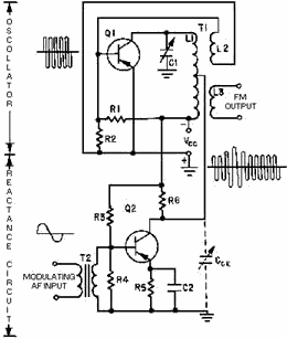
Figure 2-12. - Reactance-semiconductor FM modulator. When the modulating signal is applied to the base of Q2, the emitter-to-base bias varies at the
modulation rate. This causes the collector voltage of Q2 to vary at the same modulating rate. When the collector
voltage increases, output capacitance CCE decreases; when the collector voltage decreases, CCE increases. An
increase in collector voltage has the effect of spreading the plates of CCE farther apart by increasing the width
of the barrier. a decrease of collector voltage reduces the width of the pn junction and has the same effect as
pushing the capacitor plates together to provide more capacitance. When the output capacitance decreases,
the instantaneous frequency of the oscillator tank circuit increases (acts the same as if C1 were decreased). When
the output capacitance increases, the instantaneous frequency of the oscillator tank circuit decreases. This
decrease in frequency produces a lower frequency in the output because of the shunting effect of CCE. Thus, the
frequency of the oscillator tank circuit increases and decreases at an audio frequency (AF) modulating rate. The
output of the oscillator, therefore, is a frequency modulated RF signal.
Since the audio modulation causes the collector voltage to increase and decrease, an AM component is
induced into the output. This produces both an FM and AM output. The amplitude variations are then removed by
placing a limiter stage after the reactance modulator and only the frequency modulation remains. Frequency
multipliers or mixers (discussed in chapter 1) are used to increase the oscillator frequency to the desired output
frequency. For high-power applications, linear RF amplifiers are used to increase the steady-amplitude signal to a
higher power output. With the initial modulation occurring at low levels, FM represents a savings of power when
compared to conventional AM. This is because FM noise-reducing properties provide a better signal-to-noise ratio
than is possible with AM.
2-18
Multivibrator Modulator. - Another type of frequency modulator is the astable
multivibrator illustrated in figure 2-13. Inserting the modulating AF voltage in series with the base-return of
the multivibrator transistors causes the gate length, and thus the fundamental frequency of the multivibrator, to
vary. The amount of variation will be in accordance with the amplitude of the modulating voltage. One requirement
of this method is that the fundamental frequency of the multivibrator be high in relation to the highest
modulating frequencies. a factor of at least 100 provides the best results.

Figure 2-13. - Astable multivibrator and filter circuit for generating an FM carrier. Recall that a multivibrator output consists of the fundamental frequency and all of its harmonics.
Unwanted even harmonics are eliminated by using a SYMMETRICAL MULTIVIBRATOR circuit, as shown in figure 2-13. The
desired fundamental frequency, or desired odd harmonics, can be amplified after all other odd harmonics are
eliminated in the LCR filter section of figure 2-13. a single frequency- modulated carrier is then made available
for further amplification and transmission. Proper design of the multivibrator will cause the frequency
deviation of the carrier to faithfully follow (referred to as a "linear" function) the modulating voltage. This is
true up to frequency deviations which are considerable fractions of the fundamental frequency of the
multivibrator. The principal design consideration is that the RC coupling from one multivibrator transistor base
to the collector of the other has a time constant which is greater than the actual gate length by a factor of 10
or more. Under these conditions, a rise in base voltage in each transistor is essentially linear from cutoff to
the bias at which the transistor is switched on. Since this rise in base voltage is a linear function of time, the
gate length will change as an inverse function of the modulating voltage. This action will cause the frequency to
change as a linear function of the modulating voltage. The multivibrator frequency modulator has the
advantage over the reactance-type modulator of a greater linear frequency deviation from a given carrier
frequency. However, multivibrators are limited to frequencies below about 1 megahertz. Both systems are subject to
drift of the carrier frequency and must, therefore, be stabilized. Stabilization may be accomplished by modulating
at a relatively low frequency and translating by heterodyne action to the desired output frequency, as shown in
figure 2-14. a 1-megahertz signal is heterodyned with 49 megahertz from the crystal-controlled oscillator to
provide a stable 50-megahertz output from the mixer. If a suitably stable heterodyning oscillator is used, the
frequency stability can be greatly improved. For instance, at the frequencies shown in figure 2-14, the 2-19
stability of the unmodulated 50-megahertz carrier would be 50 times better than that which harmonic
multiplication could provide.

Figure 2-14. - Method for improving frequency stability of FM system. Varactor FM Modulator. - Another FM modulator which is widely used in transistorized circuitry uses a
voltage-variable capacitor (VARACTOR). The varactor is simply a diode, or PN junction, that is designed to have a
certain amount of capacitance between junctions. View (A) of figure 2-15 shows the varactor schematic symbol. a
diagram of a varactor in a simple oscillator circuit is shown in view (B). This is not a working circuit, but
merely a simplified illustration. The capacitance of a varactor, as with regular capacitors, is determined by the
area of the capacitor plates and the distance between the plates. The depletion region in the varactor is the
dielectric and is located between the p and n elements, which serve as the plates. Capacitance is varied in the
varactor by varying the reverse bias which controls the thickness of the depletion region. The varactor is so
designed that the change in capacitance is linear with the change in the applied voltage. This is a special design
characteristic of the varactor diode. The varactor must not be forward biased because it cannot tolerate much
current flow. Proper circuit design prevents the application of forward bias.
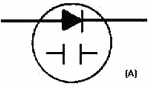
Figure 2-15A. - Varactor symbol and schematic. SCHEMATIC SYMBOL. 2-20
| - |
Matter, Energy,
and Direct Current |
| - |
Alternating Current and Transformers |
| - |
Circuit Protection, Control, and Measurement |
| - |
Electrical Conductors, Wiring Techniques,
and Schematic Reading |
| - |
Generators and Motors |
| - |
Electronic Emission, Tubes, and Power Supplies |
| - |
Solid-State Devices and Power Supplies |
| - |
Amplifiers |
| - |
Wave-Generation and Wave-Shaping Circuits |
| - |
Wave Propagation, Transmission Lines, and
Antennas |
| - |
Microwave Principles |
| - |
Modulation Principles |
| - |
Introduction to Number Systems and Logic Circuits |
| - |
- Introduction to Microelectronics |
| - |
Principles of Synchros, Servos, and Gyros |
| - |
Introduction to Test Equipment |
| - |
Radio-Frequency Communications Principles |
| - |
Radar Principles |
| - |
The Technician's Handbook, Master Glossary |
| - |
Test Methods and Practices |
| - |
Introduction to Digital Computers |
| - |
Magnetic Recording |
| - |
Introduction to Fiber Optics |
| Note: Navy Electricity and Electronics Training
Series (NEETS) content is U.S. Navy property in the public domain. |
|