Module 12 − Modulation Principles
Pages i,
1−1,
1−11,
1−21,
1−31,
1−41,
1−51,
1−61,
1−71,
2−1,
2−11,
2−21,
2−31,
2−41,
2−51,
2−61,
3−1,
3−11,
3−21,
3−31, AI−1, Index, Assignment 1, 2
frequencies in the
composite envelope. In the following analysis, vectors will be scaled to indicate the peak voltage value of the
frequencies they represent. The analysis has been simplified further by using a frequency of 8 hertz to
represent the carrier frequency. Each cycle of the carrier then requires 1/8 of a second to complete 360 degrees.
The carrier will be 100-percent modulated by a sine wave having a frequency of 1 hertz, thereby producing sideband
frequencies of 7 and 9 hertz. Envelope Development from Vectors. - The modulating signal, upper sideband,
carrier, and lower sideband waveforms are illustrated in views (A) through (D), respectively, in figure 1-43.
Notice that the vertical lines passing through the figure divide each waveform into segments of 1/8 of a second
each. These lines also coincide with the starting and ending points of each cycle of the carrier wave. 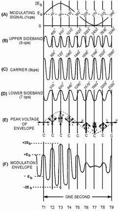
Figure 1-43. - Formation of the modulation envelope by the addition of vectors representing the
carrier and sidebands. 1-51
During the first 1/8 of a second (T1 to T2), the carrier wave completes exactly 1 cycle, or 360
degrees, as shown in view (C). The upper sideband, which has a frequency of 9 hertz, will complete each cycle in
less than 1/8 of a second. Therefore, during the time required for the carrier to complete 1 cycle of 360 degrees,
the upper sideband [view (B)] is able to complete 1 cycle of 360 degrees plus an additional 45 degrees of the next
cycle, for a total of 405 degrees. The lower sideband [view (D)] has a frequency of 7 hertz and cannot
complete an entire cycle in 1/8 of a second. During the time interval required for the carrier wave to progress
through 360 degrees, the lower sideband frequency of 7 hertz can complete only 315 degrees, 45 degrees short of a
full cycle. Keeping these factors in mind, you should be able to see that the phase angles between the two
sideband frequencies, and between each sideband frequency and the carrier frequency, will continually shift. At an
instant in time (T3), the carrier and sidebands will be in phase [view (E)], causing the envelope amplitude
[view (F)] to be twice the amplitude of the carrier. At another instant in time (T7), the sidebands are out of
phase with the carrier [view (E)], causing complete cancellation of the RF voltage. The envelope amplitude will
become 0 at this point. You should see that, although the carrier and sideband frequencies have constant
amplitudes, the ever-changing phase differences between them causes the modulation envelope to vary continuously
in amplitude. The vector analysis of the modulation envelope will be developed with the aid of figure
1-44. In figure 1-44, view (A), a vertical vector (C) has been drawn to represent the carrier wave in figure 1-43.
At T1 in figure 1-43, the upper and lower sideband frequencies are of opposite phase with respect to each other,
and 90 degrees out of phase with respect to the carrier. This condition is illustrated in figure 1-44, view (A),
by sideband vectors U and L drawn in opposite directions along the horizontal axis. Since the upper sideband U is
equal in amplitude but opposite in phase to lower sideband L, the two sideband voltages cancel one another; the
amplitude of the envelope at T1 is equal to the amplitude of the carrier. The same vector diagram is shown on a
smaller scale in figure 1-43, view (E). 
Figure 1-44A. - Vector diagrams for T1 and T2. During the 1/8 of a second time interval between T1 and T2, all three vectors rotate in a counterclockwise
direction at a velocity determined by their respective frequencies. The vector representing the carrier, for
example, has made one complete rotation of 360 degrees and is back in its original position, as shown in figure
1-44, view (B). The upper sideband frequency, however, will complete 405 degrees in this same 1/8 of a second.
Notice in view (B) that vector U has made one complete counterclockwise rotation of 360 degrees, plus an
additional 45 degrees for a total rotation of 1-52
405 degrees. Vector L, representing the lower sideband, rotates at a velocity less than that of either
the carrier or the upper sideband. In 1/8 of a second, vector L completes only 315 degrees, which is 45 degrees
short of one complete rotation. At the end of 1/8 of a second, the three vectors have advanced to the positions
shown in view (B).
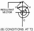
Figure 1-44B. - Vector diagrams for T1 and T2. The resultant vector in view (B) is obtained by adding vector U to vector L. Since each sideband has
one-half the amplitude of the carrier, and the two sidebands differ in phase by 90 degrees, the amplitude of the
resultant vector can be computed. This computation (not shown) would show the resultant vector to have an
amplitude that is approximately 70 percent that of the carrier. Thus, at T2 the amplitude of the modulation
envelope is about 1.7 times the amplitude of the carrier. This condition is shown in figure 1-43, view (F). By a similar procedure, vector diagrams can be constructed for time intervals T3 through T9. This has been done in
figure 1-43, view (E). From these nine individual vector diagrams, the complete modulation envelope in figure
1-43, view (F), can be constructed.
Notice in particular the vector diagrams for T3 and T7. At T3, all three waves, and therefore all three
vectors, are in phase. The modulation envelope at this instant must, therefore, be equal to twice the amplitude of
the carrier since each sideband frequency has one-half the amplitude of the carrier. At T7, the two
sideband frequencies are in phase with each other but 180 degrees out of phase with the carrier. This causes the
combined sideband voltage to cancel the carrier voltage, and the modulation envelope becomes 0 at that instant.
Note that for the transmitter output to be 0 at T7, both the carrier and sideband frequencies must be present. If
any one of these three frequencies were missing, complete cancellation would not occur and RF energy would be
present in the output. Although this vector analysis was made for frequencies of 7, 8, and 9 hertz, the
same description could be applied to the frequencies actually present at the output of a transmitter.
Modulation Level of an AM Wave As stated earlier, the modulating signal can be introduced into
any active element of a tube. In addition to the various arrangements possible within a single stage, the
modulating signal can also be applied to any of the RF stages in the transmitter. For example, the modulating
signal could be applied to the control grid or plate of one of the intermediate power amplifiers. A
modulator circuit is usually placed into one of two categories, high- or low-level modulation. Circuits are
categorized according to the level of the carrier wave at the point in the system where the 1-53
modulation is applied. The FCC defines High-LEVEL MODULATION in the Code of Federal Regulations as
"modulation produced in the plate circuit of the last radio stage of the system." This same document defines
Low-LEVEL MODULATION as "modulation produced in an earlier stage than the final." Q-36. What is
percent of modulation?
Q-37. With a single modulating tone, what is the amplitude of the sideband frequencies at 100-percent
modulation? Q-38. What is the formula for percent of modulation? Q-39. What is high-level
modulation?
MODULATION Systems To complete your understanding of AM modulation, we are now
going to analyze the operation of a typical plate modulator. Detailed circuit descriptions will be used to give
you an understanding of a basic AM plate modulator. In addition, we will cover basic circuit descriptions for
cathode and grid electron- tube modulators and for base, emitter, and collector transistor modulators in this
chapter. Plate Modulator Figure 1-45 is a basic plate-modulator circuit. Plate
modulation permits the transmitter to operate with high efficiency. It is the simplest of the modulators available
and is also the easiest to adjust for proper operation. The modulator is coupled to the plate circuit of the final
RF amplifier through the modulation transformer. For 100-percent modulation, the modulator must supply enough
power to cause the plate voltage of the final RF amplifier to vary between 0 and twice the dc operating plate
voltage. The modulator tube (V2) is a power amplifier biased so that it operates class A. The final RF power
amplifier (V1) is biased in the nonlinear portion of its operating range (class C). This provides for efficient
operation of V1 and produces the necessary heterodyning action between the RF carrier and the af modulating
frequencies. 1-54
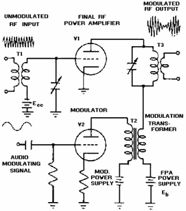
Figure 1-45. - Plate-modulation circuit.
PLATE Modulator Circuit Operation. - Figure 1-46, views (A) through (E), shows the waveforms
associated with the plate-modulator circuit shown in figure 1-45. Refer to these two figures throughout the
following discussion.
1-55
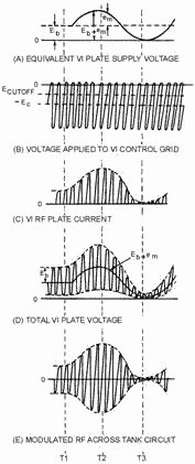
Figure 1-46. - Plate-modulator waveforms. The RF power amplifier (V1) acts as a class C amplifier when no modulation is present in the plate
circuit. V2 is the modulator which transfers the modulating voltage to the plate circuit of V1. Let's see how this
circuit produces a modulated RF output. View (A) of figure 1-46 shows the plate supply voltage for V1 as a
constant dc value (Eb) at time 1 with no modulating signal applied. V1 is biased at cutoff at this time. The
incoming RF carrier [view (A)] is applied to the grid of V1 by transformer T1 and causes the plate circuit current
to PULSE (SURGE)
1-56
each time the grid is driven positive. These RF pulses are referred to as current pulses and are shown
in view (C). The plate tank output circuit (T3) is shocked into oscillation by these current pulses and the RF
output waveform shown in view (E) is developed. The RF plate voltage waveform is shown in view (D). An
audio-modulating voltage applied to the grid of V2 is amplified by the modulator and coupled to the plate of V1 by
modulation transformer T2. The secondary of T2 is in series with the plate-supply voltage (E) of V1. The
modulating voltage will either add to or subtract from the plate voltage of V1. This is shown in view (A) at time
2 and time 3. At time 2 in view (A), the plate supply voltage for V1 increases to twice its normal value and the
RF plate current pulses double, as shown in view (C). At time 3 in view (A), the supply voltage is reduced to 0
and the RF plate current decreases to 0, as shown in view (C). These changes in RF plate current cause RF tank T3
voltage to double at time 2 and to decrease to 0 at time 3, as shown in view (E). This action results in the
modulation envelope shown in view (E) that represents 100-percent modulation. This is transformer-coupled out of
tank circuit T3 to an antenna. Because of the oscillating action of tank circuit T3, V1 has to be rated to handle
at least four times its normal plate supply voltage (Eb), as shown by the plate voltage waveform in view (D). Heterodyning the audio frequency intelligence from the modulator (V2) with the carrier in the plate circuit of the
final power amplifier (V1) requires a large amount of audio power. All of the power or voltage that contains the
intelligence must come from the modulator stage. This is why plate modulation is called high-level modulation. The heterodyning action in the plate modulator effectively changes an audio frequency to a different part of the
frequency spectrum. This action allows antennas and equipment of practical sizes to be used to transmit the
intelligence. Now, let's look at several other typical modulators.
Collector-Injection Modulator The Collector-INJECTION Modulator is the transistor
equivalent of the electron-tube AM plate modulator. This transistor modulator can be used for low-level or
relatively high-level modulation. It is referred to as relatively high-level modulation because, at the present
time, transistors are limited in their power-handling capability. As illustrated in figure 1-47, the circuit
design for a transistor collector- injection modulator is very similar to that of a plate modulator. The
collector-injection modulator is capable of 100-percent modulation with medium power-handling capabilities. 1-57
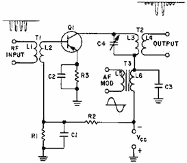
Figure 1-47. - Collector-injection modulator. In figure 1-47, the RF carrier is applied to the base of modulator Q1. The modulating signal is applied to
the collector in series with the collector supply voltage through T3. The output is then taken from the secondary
of T2. With no modulating signal, Q1 acts as an RF amplifier for the carrier frequency. When the modulation signal
is applied, it adds to or subtracts from the collector supply voltage. This causes the RF current pulses of the
collector to vary in amplitude with the collector supply voltage. These collector current pulses cause
oscillations in the tank circuit (C4 and the primary of T2). The tank circuit is tuned to the carrier frequency.
During periods when the collector current is high, the tank circuit oscillates strongly. At times when the
collector current is small, or entirely absent, little or no energy is supplied to the tank and oscillations
become weak or die out. Thus, the modulation envelope is developed as it was in a plate modulator. As
transistor technology continues to develop, higher power applications of transistor collector- injection
modulation will be employed. Plate and collector-injection modulation are the most commonly used types of
modulation because the modulating signal can be applied in the final stages of RF amplification. This allows the
majority of the RF amplifier stages to be operated class C for maximum efficiency. The plate and
collector-injection modulators also require large amounts of AF modulating power since the modulator stage must
supply the power contained in the sidebands. Q-40. For what class of operation is the final RF power
amplifier of a plate-modulator circuit biased? Q-41. The modulator is required to be what kind of a
circuit stage in a plate modulator?
Q-42. How much must the FPA plate current vary to produce 100-percent modulation in a plate modulator?
1-58
Q-43. The collector-injection modulator is similar to what type of tube modulator? Control-Grid Modulator In cases when the use of a minimum of AF modulator power is
desired, a form of low-level modulation is necessary. The CONTROL-GRID Modulator is used widely in portable and
mobile equipment to reduce size and power requirements. It is also used in extremely high-power, wideband
equipment such as television transmitters where high-level or plate modulation is difficult and costly to achieve.
Figure 1-48 is a basic schematic for a typical control-grid modulator. 
Figure 1-48. - Control-grid modulator. The control-grid modulator uses a variation of grid bias (at the frequency of the modulating signal) to
vary the instantaneous plate voltage and current. These variations cause modulation of the carrier frequency. The
carrier frequency is introduced through coupling capacitor Cc. The modulating frequency is introduced in series
with the grid bias through T1. As the modulating signal increases and decreases (positive and negative), it will
add to or subtract from the bias on RF amplifier V1. This change in bias causes a corresponding change in plate
voltage and current. These changes in plate voltage and current add vectorially to the carrier frequency and
provide a modulation envelope in the same fashion as does the plate modulator. Since changes in the plate circuit
of the RF amplifier are controlled by changes in the grid bias, the gain of the tube requires only a low-level
modulating signal. Even when the input signals are at these low levels, occasional modulation voltage peaks will
occur that will cause V1 to saturate. This creates distortion in the output. Care must be taken to bias the RF
amplifier tube for maximum power out 1-59
while maintaining minimum distortion. The power to develop the modulation envelope comes from the RF
amplifier. Because the RF amplifier has to be capable of supplying this additional power, it is biased for (and
driven by the carrier frequency at) a much lower output level than its rating. This reduced efficiency is
necessary during nonmodulated periods to provide the tube with the power to develop the sidebands. Compared to plate modulation, grid modulation is less efficient, produces more distortion, and requires the RF
power amplifier to supply all the power in the output signal. Grid modulation has the advantage of not requiring
much power from the modulator.
Base-Injection Modulator The Base-INJECTION Modulator is similar to the control-grid modulator in electron-tube circuits. It is used to
produce low-level modulation in equipment operating at very low power levels. In figure 1-49, the bias on
Q1 is established by the voltage divider R1 and R2. With the RF carrier input at T1, and no modulating signal, the
circuit acts as a standard RF amplifier. When a modulating signal is injected through C1, it develops a voltage
across R1 that adds to or subtracts from the bias on Q1. This change in bias changes the gain of Q1, causing more
or less energy to be supplied to the collector tank circuit. The tank circuit develops the modulation envelope as
the RF frequency and AF modulating frequency are mixed in the collector circuit. Again, this action is identical
to that in the plate modulator. 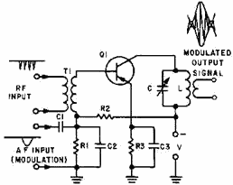
Figure 1-49. - Base-injection modulator. Because of the extremely low-level signals required to produce modulation, the base-injection modulator is
well suited for use in small, portable equipment, such as "walkie-talkies," and test equipment. Cathode Modulator Another low-level modulator, the CATHODE Modulator, is generally
employed where the audio power is limited and distortion of the grid-modulated circuit cannot be allowed. The
cathode
1-60
| - |
Matter, Energy,
and Direct Current |
| - |
Alternating Current and Transformers |
| - |
Circuit Protection, Control, and Measurement |
| - |
Electrical Conductors, Wiring Techniques,
and Schematic Reading |
| - |
Generators and Motors |
| - |
Electronic Emission, Tubes, and Power Supplies |
| - |
Solid-State Devices and Power Supplies |
| - |
Amplifiers |
| - |
Wave-Generation and Wave-Shaping Circuits |
| - |
Wave Propagation, Transmission Lines, and
Antennas |
| - |
Microwave Principles |
| - |
Modulation Principles |
| - |
Introduction to Number Systems and Logic Circuits |
| - |
- Introduction to Microelectronics |
| - |
Principles of Synchros, Servos, and Gyros |
| - |
Introduction to Test Equipment |
| - |
Radio-Frequency Communications Principles |
| - |
Radar Principles |
| - |
The Technician's Handbook, Master Glossary |
| - |
Test Methods and Practices |
| - |
Introduction to Digital Computers |
| - |
Magnetic Recording |
| - |
Introduction to Fiber Optics |
| Note: Navy Electricity and Electronics Training
Series (NEETS) content is U.S. Navy property in the public domain. |
|