|
|
|||||||||
| Software: RF Cascade Workbook | RF Symbols for Office | RF Symbols & Stencils for Visio | Espresso Workbook | ||||||||||
|
|||||||||||||||||||||||||||||||
   |
   |
||||||||||||||||||||||||||||||
|
Please Support RF Cafe by purchasing my ridiculously low-priced products, all of which I created. RF & Electronics Symbols for Visio RF & Electronics Symbols for Office RF & Electronics Stencils for Visio T-Shirts, Mugs, Cups, Ball Caps, Mouse Pads These Are Available for Free |
|||||||||||||||||||||||||||||||

Microwave Power Diodes
July 1969 Electronics World

|
July 1969 Electronics World  Table of Contents
Wax nostalgic about and learn from the history of early electronics. See articles from Electronics World, published May 1959 - December 1971. All copyrights hereby acknowledged. |
Everyone who is interested enough in microwave diodes to read this article surely knows* what IMPATT, GUNN, and PIN diodes are, but have you heard of Read-effect, TRAPATT (TRApped Plasma And Transit Time*), LSA (Limited Space-charge Accumulation), or QMD (Quenched Multiple-Domain Mode) diodes? If not, it is likely because you entered the microwaves field long after 1969 when this edition of Electronics World was mailed to subscribers. Device improvement and obsolescence accounts for familiarity with the former and unfamiliarity with the latter, respectively. The article below by two Sylvania Electronic Products engineers describes the properties of various up-and-coming semiconductor types that promised operation into the 70 GHz region.
* Stop calling me "Shirley" ;-)
** Now referred to as Trapped Plasma Avalanche Triggered Transit
This edition of Electronics World ran a series of diode articles: Hot Carrier Diodes, Variable-Capacitance Diodes, Tunnel Diodes, Microwave Power Diodes, A Survey of Silicon Junction Diodes, and Light-Emitting Diodes.
Microwave Power Diodes
Dr. Niblack (top) received his B.A. from the University of Buffalo, his A.M. in Physics from Harvard, and his Ph.D. from State University of New York. He joined Sylvania in 1961 and for three years carried out analysis of antennas and receiver systems for high frequency, microwave, and optical use and worked on the effects of radiation in semiconductors. From 1965 to 1967 he was with Motorola where he developed designs and processing for advanced MOS devices in power transistors. He rejoined Sylvania in the Semiconductor Division in 1967. He taught physics at two universities.
Mr. Levi (bottom) holds a B.A. in chemistry from University of Southern California. After two years of graduate work in chemistry, he joined Pacific Semiconductor. He has also been associated with Clevite Transistor Co. and Raytheon. He joined the staff of the Microwave Division of Sylvania in 1967. He holds several patents in the field.
By Walter K. Niblack and Clifford A. Levi
Microwave Dept., Semiconductor Div., Sylvania Electric Products
New avalanche and transferred-electron (bulk) devices, such as Read-effect or IMPATT, TRAPATT, Gunn-effect, and LSA diodes, are making possible the production. of microwave power output at frequencies above 50,000 MHz.
Ever since the invention of the transistor, people in the microwave-systems business have dreamed of being able to produce and modulate microwave power without the use of vacuum tubes such as klystrons, magnetrons, and traveling-wave amplifiers. A solid-state transmitter, which shared the advantages of solid-state circuitry at lower frequencies - chiefly small size, high reliability, high efficiency, and the elimination of multiple power supplies - was the goal.
The first practical solid-state microwave sources appeared about ten years ago and, typically, consisted of a v.h.f. transistor oscillator whose output was fed into several stages of frequency doublers using the nonlinear capacitance of varactor diodes. At first, these sources were quite inefficient and very complicated, but had good reliability. Improvements in transistor and varactor design allowed the use of one v.h.f. power transistor, together with a high-order varactor multiplier (e.g., one whose output frequency is 5 to 15 times the input frequency). This simplified the circuit considerably, but usually reduced efficiency.
Fig. 1 - (A) Cross-section schematic diagram and (B) typical impurity profile of an avalanche-type diode.
It was recognized that what was really needed was a device which, like a klystron or magnetron, would produce output at some microwave frequency with only d.c. input power, just as a transistor oscillator does at lower frequencies. Transistors have improved considerably in the past ten years and now there are some capable of producing 5 watts at 2 GHz; but, at present, these are hard to make and thus expensive. It appears to be nearly impossible in the foreseeable future to make transistors that oscillate well above 8 GHz because of basic limitations.
In the past two years, however, two new classes of diode devices have emerged which make it unnecessary to use transistors at all in many oscillator and amplifier applications above 1 GHz. These are the avalanche-type devices which may be used either as oscillators or as negative-resistance amplifiers; and the transferred-electron devices which so far have found practical application only as oscillators. Within each class there are a number of different "modes" or types of operation possible. Although it is usually necessary to optimize a given device design according to the intended mode and frequency desired, a particular device can often be operated in several different modes as circuit conditions and d.c. input are varied.
Devices in both these classes have produced power at frequencies above 50 GHz, far above the probable upper limit for transistors. Being two-terminal devices, they require only very simple d.c. power supplies and no bias on a third terminal. Also, both types will oscillate in the transit-time mode in almost any high-"Q" cavity if efficiency is not important.
Fig. 2 - By using diamond as part of the heat sink, the thermal performance of avalanche diode is improved.
Table 1 - Partial listing of some available IMPATT diodes.
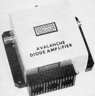
Fig. 3 - Three-stage avalanche-diode amplifier package.
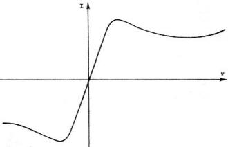
Fig. 4 - Typical I-V curve for bulk gallium arsenide showing the negative resistance above certain voltage.
There is some confusion about the modes since various manufacturers have given different names to the same mode. For the avalanche devices, there are three recognized modes: (1) the Read-effect, or transit time, or IMPATT (IMPact ionization And Transit Time) mode; (2) the "anomalous," or subharmonic, or TRAPATT (TRApped Plasma And Transit Time) mode; and (3) the self-pumped parametric mode. There are four clearly recognized modes for transferred-electron (bulk) devices: (1) the Gunn-effect, or transit-time mode, (2) the delayed-domain mode, (3) the LSA (Limited Space-charge Accumulation) mode, and (4) the QMD (quenched multiple-domain mode). Since both types of device exhibit complicated behavior, it is possible that other modes will be identified in the future.
With solid-state sources available to convert d.c. directly to microwave r.f., some means is required to modulate the output. Simply varying the d.c. input will do the trick, but in optimized circuits this results in simultaneous changes in both frequency and amplitude, so other means are desirable. If frequency modulation is desired, the best solution is to apply the modulating voltage to a tuning varactor coupled to the oscillator circuit. (These diodes are covered in another article in this Special Section.)
If amplitude modulation or pulse modulation is desired, it has been the practice for a number of years to use p-i-n diodes. These diodes can be used as current-variable attenuators in forward bias, but their primary use is as switches for pulse modulation and phase shifting. As high-speed switches, they can also handle very large amounts of incident power (up to 10 kW pulsed power and hundreds of watts c.w.) because of their low loss in both the "on" and "off" states, and high breakdown voltage.
Avalanche Diodes
The avalanche IMPATT diode is a two-terminal negative-resistance device which can be fabricated of silicon, germanium, or gallium arsenide and is shown in Fig. 1A. The indicated p+ region may be formed by diffusion, epitaxial growth, or ion implantation; the first being most common.
When the diode is reverse-biased into breakdown, the depleted n zone is functionally divided into two regions; an avalanche region and a drift region. In the avalanche region, the field is high enough to cause impact ionization, which causes continual production of free electrons and holes. This is strongly dependent on the field within the region. An increase in field causes an increase in the rate of change in the number of electron-hole pairs, and thus the current. There is a phase shift between the voltage and current so the avalanche current acts inductively. A further phase shift occurs across the drift region. If at some frequency the total phase shift for the two regions is greater than 90°, the diode exhibits a negative resistance at that frequency. This picture is complicated by the fact that capacitive (displacement) current also flows in the avalanche and drift regions causing a resonance.
The n+ region serves as a contact for the active region of the diode and as a support during fabrication of the slice.
Typically, these diodes are mesa structures. An X-band diode might have a mesa diameter of 3-5 mils and an impurity distribution as shown in Fig. 1B.
Since typical efficiencies in the IMPATT mode are on the order of 10% or less, an input power of over 10 watts is required for 1-watt output, at say 10 GHz. At least 9 watts must therefore be dissipated. Hence, the thermal design is extremely important. For this reason, avalanche diodes are mounted with the anode bonded to a diamond heat sink to reduce the distance from the junction to the heat sink. Fig. 2 is a drawing of a diode bonded to a diamond heat sink. Diamond is a better heat conductor than copper by a factor of four and advantage is taken of this in the critical spreading region of the heat path. Proper thermal design can permit thermal resistances of less than 6°C/W for a junction diameter of 5 mils, as opposed to typically 15°C/W for the chip mounted directly on copper.
In operation, as current is increased, a threshold current is reached, the value of which depends on diode area, frequency, and doping of the avalanche region. For a diode which is not thermally limited, the output power then increases with input power to a saturation value. The efficiency also increases with input power to near the saturation point. Hence, for maximum efficiency, a diode must be designed to operate optimally at its design power level.
Waveguide circuit.
Coaxial circuit with adjustable transformer sections.
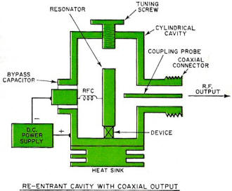
Re-entrant cavity with coaxial output.
Three circuit configurations that have been used for avalanche and transferred-electron device oscillators, The d.c. power supply should be of the regulated-current type with avalanche diodes. Voltage, current, and polarity depend on device.
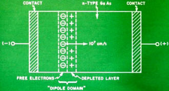
Fig. 5 - Gunn diode showing the traveling domain produced.
Fig. 6 - A practical Gunn diode structure is shown here.
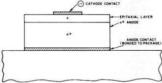
Fig. 7 - Operation of "p-i-n" diode with forward-bias.
The performance of an IMPATT diode depends critically upon the design of the circuit in which it is operated. Efficient operation has been achieved in waveguide cavities, coaxial cavities, stripline, and microstrip circuits. In the design of a circuit, attention must not only be given to the impedance presented to the diode at the fundamental frequency, but, in oscillator applications, to the proper terminations of the harmonics.
In the laboratory, power output at X-band of approximately 2 watts c.w. has been obtained in a single-chip device operating as an oscillator in the IMPATT mode. Similarly, multiple-chip devices have been built which generate as much as 5 watts c.w. Frequencies covered have ranged from 500 MHz to 70 GHz with 100-mW output being achieved in the laboratory at 50 GHz.
In the TRAPATT mode, much higher powers and efficiencies have been achieved. Five watts c.w , at 40% efficiency has been reported for a single chip. In pulsed operation, much higher powers, on the order of a hundred watts at 40% or higher efficiency, have been reported. These results are generally at frequencies below X-band but, in principle, similar efficiencies could be achieved at X-band. There is little doubt that performance such as that just cited will move out of the lab and into the market place in the near future.
For the present, both IMPATT diodes and complete oscillator circuits are commercially available from a number of sources and at power levels up to 1 watt at X-band. Table 1 is a partial listing of available diodes and oscillators. Since the field is moving so rapidly, it is difficult to prepare an exhaustive list. In addition to oscillator circuits, a 3-stage amplifier is available from Sylvania. This device, shown in the photograph, Fig. 3, provides 40-dB gain with up to 200-mW output.
Single diode circulator-coupled avalanche amplifiers have been built with outputs over one watt in the X-band, and bandwidths over 2.5 GHz reported, using commercial diodes.
Transferred-Electron (Bulk) Devices
The transferred-electron effect is an effect which occurs because of peculiarities of the conduction band in certain semiconductors such as gallium arsenide. It does not occur in semiconductors such as silicon and germanium. The effect occurs when the field in an n-type sample exceeds a certain threshold, giving the electrons enough energy to transfer to another conduction band with higher energy and lower mobility. This results in a decrease of average mobility, and thus a decrease in conductivity, as the field increases. In simple terms, bulk gallium arsenide exhibits a negative small-signal resistance above a certain voltage. A typical I-V curve is shown in Fig 4.
At first it might seem that a slab of gallium arsenide could be made to amplify, just as a tunnel diode does, simply by connecting it to a positive-resistance load nearly equal in magnitude to the negative resistance and applying voltage, and that the frequency of operation would he determined entirely by a cavity or a tuned circuit. However, if an excess of electrons is created somewhere, instead of diffusing away from each other as usual, they diffuse toward each other leaving behind positively charged donor atoms. This segregation of positive and negative charges is a "dipole domain."
As soon as ohmic contacts arc made to a piece of gallium arsenide, and sufficient field is applied, electrons are injected at the negative end and a domain immediately forms.
The electrons in the domain are free to move toward the anode so the whole domain drifts toward the anode at a velocity of about 107 cm/second. This is shown in Fig. 5. Since most of the voltage drop is taken up by the domain, no new domain can form until the existing one is destroyed at the anode, allowing the bulk field to rise into the negative-resistance region again.
For this reason, the sample oscillates at a natural frequency (f0) close to 107/L (where L is the cathode-anode spacing in centimeters), regardless of circuit conditions. In practice, it is possible to "pull" the oscillation frequency from its natural value, f0 by ±10% by coupling to an external high-"Q" cavity.
Fabrication of practical Gunn diodes is complicated by the fact that the value of L must be small (about 10 microns for f0 = 10 GHz) so that the device cannot be made by the obvious procedure of putting ohmic contacts on opposite sides of a single crystal slab of thickness L. Epitaxial layers of lightly doped gallium arsenide on heavily doped substrates must be used. In addition, the doping must be very light and very uniform if high conversion efficiency is desired. It is very difficult to meet these conditions, hence Gunn diodes are expensive to make. The structure of a practical Gunn device is shown in Fig. 6.
In modes other than the Gunn mode, the creation and annihilation of domains is controlled by material properties or circuit waveforms. In the LSA mode, domains are virtually completely suppressed by increasing crystal thickness and reducing doping level, while improving uniformity (very difficult). Because gallium arsenide is a poor heat conductor, and high input powers must be used, LSA devices must be pulsed.
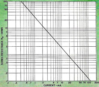
Fig. 8 - Forward-bias characteristics of the "p-i-n" diode.
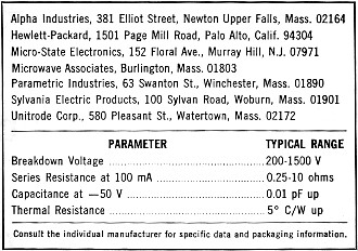
Table 2 - Partial list of suppliers of microwave "p-i-n" diodes along with typical range of operating parameters.
Operating a Gunn diode is extremely simple. The diode is placed in a circuit that resonates near f0 and d.c. voltage from a low-impedance source is applied until the field exceeds the critical field, causing domain formation. As the voltage is increased, the power output increases rapidly until the efficiency reaches a maximum of 2 to 5 percent. Power output usually continues to increase with increasing voltage until the device burns out.
A typical X-band Gunn diode might produce 20 to 50 mW output at 10 volts and 100 mA. The threshold would be about 5 volts, and burnout might occur due to overheating at as low as 12 volts.
P-I-N Diodes
The p-i-n diode, which can be made only in silicon, is basically an electronically controllable variable resistance. In some applications (switching, phase shifting) only two of its states are used, that is, "on" and "off." In others, such as attenuator or modulator, the continuous variation of resistance with forward current is utilized.
The operation of this diode depends upon the modulation of the conductivity of an intrinsic (very high resistivity) region by injection of holes and electrons under forward bias. Fig. 7 is a schematic of a p-i-n diode under forward bias. At low current levels or at zero or negative bias very few carriers exist in the i region. Since the conductivity is directly proportional to the number of carriers, the resistance of this region is high. As the current is increased, however, the conductivity increases as injected carriers from the p+ and n+ regions dope the i region. This effect is called conductivity modulation and is exhibited to some extent in all forward-biased p-n junctions when the injected carrier density becomes comparable to or exceeds the background doping. Fig. 8 is a plot of resistance vs forward current for a typical p-i-n diode. Operating bias levels for switches or phase shifters might be in the 10-150 mA range.
In the reverse direction, mobile charge is swept out of the i region and it becomes an insulating dielectric. The diode behaves as a typical reverse-biased junction with two exceptions. Since the i region has few carriers to be removed, it is swept out at low voltage and, in a good diode, punches through at a few volts or occasionally at zero bias. Since the i region is typically fairly thick, the capacitance per unit area at lower reverse voltages is less than for a comparable p-n junction.
In summary, then, a p-i-n diode can be represented as a current-variable resistance in the forward direction and as a constant capacitance in the reverse direction.
In microwave applications, the time during which the applied signal exceeds the breakdown voltage of the diode is too short for buildup of avalanche current to occur. A p-i-n diode, may, therefore, control peak r.f. voltage greater than the breakdown voltage of the diode.
In the forward-biased state, the r.f. current swing can exceed the d.c. bias without causing much rectification. Since the diode has a finite series resistance, power is dissipated and, therefore, the thermal design of the diode is important when appreciable powers are to be handled. This is particularly important in applications when the diode may not be fully conductivity modulated. Diodes should be selected with low thermal resistance as one of the criteria.
Posted March 20, 2018

Copyright: 1996 - 2026 |
About RF Cafe RF Cafe began life in 1996 as "RF Tools" in an AOL screen name web space totaling 2 MB. Its primary purpose was to provide me with ready access to commonly needed formulas and reference material while performing my work as an RF system and circuit design engineer. The World Wide Web (Internet) was largely an unknown entity at the time and bandwidth was a scarce commodity. Dial-up modems blazed along at 14.4 kbps while tying up your telephone line, and a lady's voice announced "You've Got Mail" when a new message arrived... |
Copyright 1996 - 2026 All trademarks, copyrights, patents, and other rights of ownership to images
and text used on the RF Cafe website are hereby acknowledge My Hobby Website: My Daughter's Website: |


