|
|
|||||||||
| Software: RF Cascade Workbook | RF Symbols for Office | RF Symbols & Stencils for Visio | Espresso Workbook | ||||||||||
|
|||||||||||||||||||||||||||||||
  |
   |
||||||||||||||||||||||||||||||
|
Please Support RF Cafe by purchasing my ridiculously low-priced products, all of which I created. RF & Electronics Symbols for Visio RF & Electronics Symbols for Office RF & Electronics Stencils for Visio T-Shirts, Mugs, Cups, Ball Caps, Mouse Pads These Are Available for Free |
|||||||||||||||||||||||||||||||
Light-Emitting Diodes
July 1969 Electronics
World
|
June 1969 Electronics World  Table of Contents
Wax nostalgic about and learn from the history of early electronics. See articles from Electronics World, published May 1959 - December 1971. All copyrights hereby acknowledged. |
Light-emitting diodes (LED's) were still relatively new to the scene of solid state electronics in 1969 when this article was published in Electronics World Magazine. Two engineers from RCA Electronic Components wrote to describe the state of the art in LED physics and features. The pair's prediction that the LED would become "a light source that can be used for indication and display wherever tungsten-filament, incandescent lamps are used" did not yet have enough insight into the devices to know that four decades would pass before their prediction would be realized. LED's have made continual progress over time, but it has really only been in the last decade and a half that significant advances have occurred - brought on largely by the desire to replace the "evil" Edison incandescent. If you want to follow up-to-the-minute news on LED's visit the Semiconductor Today website; I go there daily looking for headlines.
This edition of Electronics World ran a series of diode articles: Hot Carrier Diodes, Variable-Capacitance Diodes, Tunnel Diodes, Microwave Power Diodes, A Survey of Silicon Junction Diodes, and Light-Emitting Diodes.
Light-Emitting Diodes
Mr. Myers (top) is an Applications Engineer with the responsibility for evaluating, rating, and supplying technical information on RCA LED's and related products. He has been an Applications Engineer with the company for 6 years.
Mr. O'Brien (bottom) has been an RCA Product Development Engineer for seven years and has worked on a number of semiconductor programs, including thermoelectric power generation and IC's. He is currently responsible for process development and device design on commercial LED's.
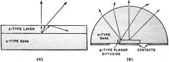
Fig. 1 - (A) Arrows show light produced in a flat-geometry gallium-arsenide diode. At an incident angle greater than 15° there is a total internal reflection and re-absorption. (B) Hemispheric-geometry LED overcomes this limitation.
By R. S. Myers and J. O'Brien
RCA Electronic Components
These significant new solid-state devices can be used for indication and display, replacing incandescent lamps in a good many applications.
The light-emitting diode, LED, a light source that can be used for indication and display wherever tungsten-filament, incandescent lamps are used, is among the most significant new semiconductor devices. Although it is still not fully developed, it is clearly destined to become the of the most commonly used semiconductors in military, industrial, and commercial electronics, as well as in consumer products, such as electrical appliances and automobiles. The LED will, by its nature, be more evident and have a greater direct effect on the consumer than the integrated circuit. In short, the LED will be seen everywhere; a bold prediction based on its usefulness, founded on the LED's inherent properties and advantages over other light sources.
The significance of the LED lies in the fact that it helps to fill a pressing need for a simple, trouble-free means of displaying information obtained by electronic equipment. At present, the output of such equipment is interpreted through pilot lamps, neon-glow readout tubes, cathode-ray tubes, and mechanical printers. Some of these devices cost more than the equipment with which they are used. The limitations of these devices are overcome by the reliable, low-power, light-emitting diode.
The solid-state construction of this diode makes it a light source virtually immune to catastrophic failure and mechanical breakdown. It eliminates the need for sockets, special power circuits, and the additional operating tests necessary to check tungsten-filament indicator lamps. LED's can be used as reliable fault or warning indicators in power-supply monitors, blown-fuse indicators, logic-circuit status indicators, battery-charge indicators, and failed-car-light indicators, to name a few applications.
Beyond these simple "on-off" indicators are the display applications: alphanumeric outputs from computers and memory systems, and various pattern readouts from such diverse devices as watches, calculators, and measuring instruments. The use of LED's in digital instruments has already been demonstrated by three firms. The future growth of these displays will be accelerated by the simple IC driver circuits already being designed.
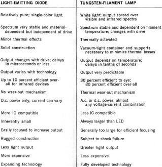
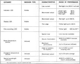
The LED's characteristics are best demonstrated by a comparison with a tungsten-filament incandescent lamp (see Table 1). Table 2 shows the wide range of LED's that can be manufactured within the present technology.
Fig. 2 - (A) Construction of LED using edge emission of light. (B) Schematic of the RCA Type 40598A LED.
LED Operation
Some semiconductor materials can be made to emit light when excited in such a manner that recombination of an electron and a hole results in the emission of a photon. Although a p-n junction is not essential for electroluminescence, since bulk materials have been made to emit light, it is still the most efficient means of generating large numbers of holes and electrons and exciting them into the energy levels needed for radiative recombination.
When a junction is forward-biased, electrons from the n region are injected into the p region where they recombine with excess holes. In the radiative process, the energy given up in a recombination is in the form of a photon whose wavelength corresponds approximately to the band-gap energy of the semiconductor. The generated photon then travels through the lattice until it is either re-absorbed by the crystal or escapes from the surface as light.
The wavelength of the emitted light is a function of the band gap of the material used for forming the junction. Pure gallium arsenide with a band gap of 1.4 electron volts emits in the near infrared region, while visible wavelengths may be obtained by using materials with larger band gaps, such as gallium phosphide (2.26 electron volts), which produces green light. When gallium phosphide is doped with zinc and oxygen, it produces red light and certain alloys of gallium arsenide emit reddish light with the actual wavelength dependent on the composition of the alloy used.
The optical power output of a device is determined, in general, by the internal geometry of the gallium-arsenide pellet and the type of package used. The simplest type of geometry is the planar or flat-geometry device in which a shallow p-type diffusion is made into an n-type substrate. Small-area contacts are applied to the p surface of the device, on a standard TO-18 header; light is generated in the p-n junction area and exits through the chip surface.
There are several limitations to the approach just described. As shown in Fig. 1A, the very high index of refraction of gallium arsenide results in a very low critical angle (15°) at the gallium-arsenide-air interface. Thus, any photons generated within the crystal which arrive at the surface with an incident angle greater than 15° are subject to total internal reflection and are usually re-absorbed within the crystal.
Table 1 - Comparative characteristics of light-emitting diodes and conventional tungsten-filament lamps.
A structure which overcomes this limitation is shown in Fig. 1B. The gallium-arsenide crystal has been ground and polished into a hemisphere and a planar p region diffused into the base. By proper choice of crystal diameter, all light originating from the region of the junction can be made to arrive at the surface of the hemisphere with an angle of incidence less than the critical angle. Thus total internal reflection is virtually eliminated. Devices fabricated by this technique exhibit efficiencies about ten times greater than planar and flat-geometry devices.
Performance similar to, but less efficient than, that of the hemispheric crystal can be obtained by covering a flat-emission chip with a dome of some material, such as epoxy, that has a high index of refraction. An epoxy with an index of refraction of about 1.5 improves the performance of uncoated devices by about 2 to 3 times.
Another method of utilizing the light generated within a crystal takes advantage of edge emission, a mode in which light is emitted from the perimeter of the device, as shown in Fig. 2A. The Type 40598A infrared emitter uses edge emission; in this device light is emitted from the perimeter of a square-mesa-type diode that is mounted in a parabolic reflecting surface, as shown in Fig. 2B. The emitting area of the diode falls within the focal plane of the parabola. An epoxy lens forms the optical window and aids in collimating the light to within 15° of the optical axis.
In the past, high costs have hindered the development of a market for devices like this. However, because costs have been steadily decreasing, the future appears promising. The fifteen-dollar-per-gram cost of gallium-arsenide wafers is still a problem, but refinements in crystal growth and better control of device fabrication processes promise to lower costs even further as a volume market begins to open up for light-emitting diodes.
LED Optical Systems
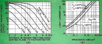
Fig. 3 - (A) Performance curve for 40598A LED having a nominal output of 1.6 mW at 50 mA. (B) Performance curve for FPM-100 detector is used next to obtain light current.
Fig. 4 - Block diagram of a pulse light system with LED.
The performance of an optical system incorporating an LED is difficult to describe primarily because there are so many variables, including LED output, alignment of LED and detector, beam spread of LED output, required detector output current, range of radiation, and ambient light level.
In a given application, many performance factors are fixed. Manufacturers of LED's and detectors provide data which makes it easy to predict the performance of an optical system when these fixed values are known. The following paragraphs describe several applications of LED's and show how their performance may be predicted. For the purposes of this article, certain assumptions will be understood; namely, that all of the output of an LED is at one wavelength, that the emitted beam of light has uniform intensity, and that all parts of the system operate at nominal values and ratings.
Optical System with Maximum. LED-to-Detector Coupling and No Lens. An optical system of this type is referred to as an optical coupler. It is used to provide voltage isolation and direct coupling of input and output; the isolation may be several thousand volts. The method of predicting the performance of such a system is as follows:
1. Look up total power received by the detector in data provided by the LED manufacturer.
2. Calculate power density on detector. Power density = [total power received (mW) ] / [detector area (cm2)].
3. Obtain expected output from detector from data supplied by the detector manufacturer. Correct data for wavelength of LED, if necessary, by using data supplied for this purpose by the manufacturer.
As an example of the use of this method in actual practice, consider the performance of an optical coupler composed of an RCA 40598A LED and a Fairchild 0.06-inch-diameter detector (Type FPM-100) separated by a distance of 0.1 inch. The steps to be followed correspond to those outlined above in the general-method description and are as follows:
1. Total power received by the detector from the manufacturer's data given in Fig. 3A is 28% X 1.6 mW = 0.45 mW.
2. Power density = 0.45 mW / π (0.03 in)2 = 159 mW/in2 or 25 mW/cm2.
3. Detector output current from manufacturer's data in Fig. 3B is about 4 milliamperes at 5 volts unadjusted for wavelength, and, applying a correction recommended by the detector manufacturer, approximately 12 milliamperes at 5 volts adjusted for wavelength.
Table 2 - This listing shows the wide range of light-emitting diodes that are now being manufactured.
Optical System with Separated LED and Detector and No Lens. A system with a separation between emitter and detector and no lens is needed for applications such as card readers, tape readers, object counters on production lines, and for simple intrusion alarms. The procedure for predicting the performance of this system is the same as for the optical coupler if a performance curve for the LED is available. For the important applications of card and tape readers, the information called for in steps 1 and 2 is available directly from the LED manufacturer.
For applications in which there is a large separation between the LED and the detector, the detector output is very small. Such a system becomes unusable when the ambient light produces more detector output than the LED. Intrusion alarms, photoelectric controls for production lines, and long-range signaling systems are plagued by ambient-light problems. Ambient light varies more than 100 million times from the dark of a movie theater to a bright sunny day and its exact level is not easily determined. Even indoors, the ambient-light level varies greatly because of window light, reflections, and shadows. Systems using LED's can be made independent of ambient light by taking advantage of the LED's high-speed pulse or high-frequency-modulation capabilities.
Pulsed and Modulated Light Systems
Pulsed or modulated light systems use detectors which respond to the pulse rise time or high-frequency modulation of the light emitted by an LED and ignore the absolute light level of the device. Tungsten lamps cannot produce high-speed pulses and therefore must be used with absolute-value detectors which require that the light of the emitting lamp be much greater than the highest ambient light expected. LED's can be used even if the ambient light is stronger than that emitted by the LED, as the following example demonstrates.
The 1 milliwatt of absolute light produced by the 40598A LED is detectable, under room-lighting conditions, at a maximum distance of 2 inches, by a detector with an area of 1 square centimeter. However, the pulsed light produced by the same device is detectable at 2 feet under room-lighting conditions even with a 10-watt tungsten lamp focused on a 5-square-millimeter detector to simulate the maximum ambient lighting conditions. A 1-microsecond pulse with a repetition rate of from 100 to 5000 Hz and a pulse power output of 6-milliwatts peak is used. A block diagram of the pulsed system is shown in Fig. 4. By comparison with the absolute method, the pulsed method shows an improvement in excess of 10 to 1 in working separation and in excess of 100 to 1 in sensitivity, and displays a far greater improvement in immunity to ambient light.
Systems with Lens
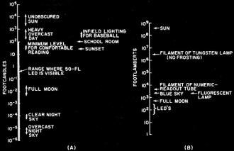
Fig. 5 - (A) Representative light intensities falling on a surface along with (B) brightness of the various sources.
A lens placed between the LED and detector, but close to the LED, can be used to direct uselessly diverging light toward the detector and thereby increase the output of the system. Similarly, a lens placed between the LED and detector, but close to the detector, focuses divergent light on the detector and effectively increases detector size to that of the lens.
Because lenses greatly increase the output of a system, they allow greater LED-to-detector separation; theoretically miles, and quite practically many yards. Clearly, the use of a lens requires that the LED and detector be precisely positioned. Positioning is often the factor which limits the effectiveness of an optical system and thereby limits the separation of LED and detector.
LED's as Indicator Lights
The human eye responds to the difference in brightness (brightness ratio) between the LED and the background. The total output and size of the LED are important in that they affect the brightness of the LED; to be seen, an LED must be noticeably brighter than its background. How much brighter depends upon the LED's color and the brightness of the actual surroundings; i.e., the amount of ambient light, a quantity that varies over a very wide range, as indicated in Fig. 5.
The range of illumination in which a 50-footlambert LED can be seen extends from approximately 100 footcandles to total darkness. A tungsten lamp with a clear bulb yields about 3 X 10⁶ footlamberts and is therefore visible under higher ambient light levels. Fig. 5 puts these ranges and levels in perspective.
The growth of the LED will be paced in the next three to five years by the development of new semiconductor materials and the refinement of processing techniques. This developmental sequence is completely analogous to the development problems and growth cycle of other semiconductor devices which used new materials and therefore new processing techniques. Perhaps the best analogy is the silicon transistor; however, the silicon transistor is a great deal more complex than the LED.
At this time, comparatively few LED's are available. Technological problems and high individual device costs related to unfinished engineering on these devices are the most important limiting factors. However, present costs cannot be related to costs five years or even one year from now. Both costs and performance will change greatly for the better in the next few years as the technology advances. Future products will include a large percentage of visible emitters, and larger, more powerful devices that will be used in a greater number of larger, brighter, and more complex displays.

Copyright: 1996 - 2026 |
About RF Cafe RF Cafe began life in 1996 as "RF Tools" in an AOL screen name web space totaling 2 MB. Its primary purpose was to provide me with ready access to commonly needed formulas and reference material while performing my work as an RF system and circuit design engineer. The World Wide Web (Internet) was largely an unknown entity at the time and bandwidth was a scarce commodity. Dial-up modems blazed along at 14.4 kbps while tying up your telephone line, and a lady's voice announced "You've Got Mail" when a new message arrived... |
Copyright 1996 - 2026 All trademarks, copyrights, patents, and other rights of ownership to images
and text used on the RF Cafe website are hereby acknowledge My Hobby Website: My Daughter's Website: |


