This content was generated by primarily
with the assistance of ChatGPT (OpenAI), and/or
Gemini (Google), and/or
Arya (GabAI), and/or Grok
(x.AI), and/or DeepSeek artificial intelligence
(AI) engines. Review was performed to help detect and correct any inaccuracies; however,
you are encouraged to verify the information yourself if it will be used for critical
applications. In all cases, multiple solicitations to the AI engine(s) was(were)
used to assimilate final content. Images and external hyperlinks have also been
added occasionally - especially on extensive treatises. Courts have ruled that AI-generated
content is not subject to copyright restrictions, but since I modify them, everything
here is protected by RF Cafe copyright. Many of the images are likewise generated
and modified. Your use of this data implies an agreement to hold totally harmless
Kirt Blattenberger, RF Cafe, and any and all of its assigns. Thank you. Here is
Gab AI in an iFrame.
AI Technical Trustability Update
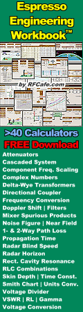
While working on an update to my
RF Cafe Espresso Engineering Workbook project to add a couple calculators about
FM sidebands (available soon). The good news is that AI provided excellent VBA code
to generate a set of Bessel function
plots. The bad news is when I asked for a
table
showing at which modulation indices sidebands 0 (carrier) through 5 vanish,
none of the agents got it right. Some were really bad. The AI agents typically explain
their reason and method correctly, then go on to produces bad results. Even after
pointing out errors, subsequent results are still wrong. I do a lot of AI work
and see this often, even with subscribing to professional versions. I ultimately
generated the table myself. There is going to be a lot of inaccurate information
out there based on unverified AI queries, so beware.
Electronics & High Tech
Companies | Electronics &
Tech Publications | Electronics &
Tech Pioneers | Electronics &
Tech Principles |
Tech Standards Groups &
Industry Associations | Societal
Influences on Technology