|
|||||||||||||
 |
|||||||||||||
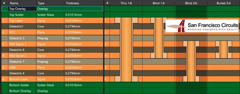
Types of PCB Vias
|
|||||||||||||

Press Release Archives: Content is copyright of company represented. Page format, custom text and images are RF Cafe copyright - do not distribute. Note: Posting of press releases costs $100 each for non-advertisers.
San Francisco Circuits: Types of PCB Vias July 11, 2025 - San Mateo, California - San Francisco Circuits has published a comprehensive guide on the 8 most essential types of PCB vias, helping designers, engineers, and procurement teams navigate the challenges of modern board manufacturing. This is a guide to the 8 different via types. As electronic devices continue to shrink in size while increasing in complexity, PCB vias play a critical role in enabling multi-layer interconnections, high-speed signal integrity, and thermal performance. The 8 Main Types of PCB Vias Each via type serves a specific function depending on the board’s structure, component density, and electrical requirements:
Why It Matters: Performance, Reliability & Manufacturability
San Francisco Circuits - Your Expert in Advanced Via Technology With expertise in fabricating complex multilayer and HDI PCBs, San Francisco Circuits offers advanced via capabilities, including:
Our engineering team can help optimize your stack-up and via strategy to meet stringent performance, size, and reliability requirements. Read more including the full breakdown on the Types of PCB Vias on the San Francisco Circuits website. About San Francisco Circuits San Francisco Circuits is a provider of PCB fabrication and assembly, has a dedicated team specializing in simple and complex PCB fabrication and assembly technologies. They can produce elaborate and high-quality PCBs in a number of custom and common layouts. From basic to intricate PCBs–their engineers will meet your PCB fabrication & assembly needs. The company provides a rare balance between technical expertise and competitive pricing. And they not only provide high-quality products but also high-quality customer service at the same time. San Francisco Circuits has been voted by National Television as the "world's greatest in PCBs" and has demonstrated experience as a power player in PCB fabrication and assembly. If you are looking to discuss PCB projects of any size or scope, feel free to reach out to them via our website (see below).
Contact Victor Bilandzic Web: www.sfcircuits.com |
|||||||||||||
 |
|||||||||||||
|
|||||||||||||


|
||||||||||||||||||||||||||||||||||||