|
|
|||||||||
| Software: RF Cascade Workbook | RF Symbols for Office | RF Symbols & Stencils for Visio | Espresso Workbook | ||||||||||
|
|||||||||||||||||||||||||||||||
   |
   |
||||||||||||||||||||||||||||||
|
Please Support RF Cafe by purchasing my ridiculously low-priced products, all of which I created. RF & Electronics Symbols for Visio RF & Electronics Symbols for Office RF & Electronics Stencils for Visio T-Shirts, Mugs, Cups, Ball Caps, Mouse Pads These Are Available for Free |
|||||||||||||||||||||||||||||||

The What and Why of Integrated Circuits
October
1963 Radio-Electronics

|
October 1963 Radio-Electronics  [Table of Contents] [Table of Contents]
Wax nostalgic about and learn from the history of early electronics. See articles from Radio-Electronics, published 1930-1988. All copyrights hereby acknowledged. |
Jack Kilby is credited with inventing the world's first integrated circuit in 1958, while working at Texas Instruments. That was a mere decade after the first transistor was made at Bell Labs. Another half a decade passed and we had the level of complexity of integrated circuits reported here in the October 1963 issue of Radio-Electronics magazine. While working at Westinghouse (now Northrup Grumman) back in the early 1980s, I used the tapped resistor and tapped capacitors on a fairly regular basis to tune RF circuits in the lower ISM bands. That involved using a thermosonic wire bonder to make the connections, then make measurements, and repeat until the frequency was where it needed to be. Those circuits used multiple ICs and discretes (mainly Rs and Cs) mounted on tiny polyimide PCB substrates which I did the layout for. The technology was used heavily by the Aerospace Electronics division adjacent to BWI Airport.
See also Integrated Circuit Techniques, The What and Why of Integrated Circuits, Evolution in Electronics: Integrated Circuits, Integrated Circuits: What's Available?, and The Integrated-Circuit Industry.
The What and Why of Integrated Circuits
 A report on the science of vanishing electronics
By Lothar Stern*
Scientists in virtually every field are striving for bigger accomplishments and larger end-products. In electronics, the best brains are going in the opposite direction. Today the emphasis is on smallness-almost to the vanishing point. The results already achieved have caused more excitement and anticipation than any development since the invention of the transistor. A new electronic technology is born - integrated circuits.
A multistage amplifier, a complete flip-flop, an elaborate computer gate, all so tiny that their individual structures can be seen only under the microscope, will be the basic tools of the electronic technician. Every phase of the industry, from engineering to servicing, from equipment production to product marketing, will feel the impact. The concept of integrated circuits heralds the beginning of a new era in the electronics art.
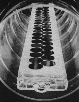
Fig. 1 - Crystal layers are grown on the basic substrate in rf furnaces like this. Gases are flowed over the induction -heated semi-conductor wafers in the quartz tube to produce the desired epitaxial surface layer.
What Are Integrated Circuits?
Even the electronics industry itself has not yet agreed on a precise definition. But a semblance of order was brought into the confusion last January. The EIA (Electronics Industry Association) proposed a definition that has at least tentative approval from a large number of manufacturers.
"Integrated circuits," proposes the EIA, "are the physical realization of a number of circuit elements inseparably associated on or within a continuous body to perform the function of a circuit."
Electronically, integrated circuits are not radically different from those in common use. They still consist of separate component parts - transistors, diodes, resistors and capacitors - interconnected to form a working whole. Physically, there is no comparison. Unlike conventional circuits, whose component parts are separately manufactured and individually packaged, integrated circuit parts are all fashioned simultaneously and with identical processes. All are deposited on or within a tiny "chip" of silicon no thicker than a page of this publication and only a few tens of thousandths of an inch square. And, in the completed circuit, these parts are neither separable nor repairable.
Why Integrated Circuits?
Integrated circuits are of major importance to the electronics industry because of their technological and economic advantages.
Small size and weight are the most obvious. Capable of being compressed into a minute volume, they are the answer to many space-age and military electronics problems. Present methods of packaging are designed more for standardization than for minimized dimensions, yet are flexible enough to meet almost any need.
Size and weight reducing capabilities are the most obvious integrated-circuit features, but by no means the most important. At least as vital is the increase in equipment reliability. Separate interconnecting wires and their solder connections are replaced with vapor-deposited metallization patterns. This promises to eliminate a major source of equipment trouble. Use of high-reliability semiconductor devices and manufacturing processes is expected to improve systems reliability further.
Finally, since a complete circuit now becomes the basic building block of electronic equipment, the number of actual parts is sharply reduced, extending the life of a complex system.
But perhaps the most important overall advantage of integrated circuits is the prospect of cost reduction. This is due not only to the small cost of the actual materials required, but also to the labor and equipment savings of the manufacturing processes.
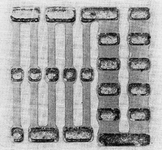
Fig. 2 - Integrated-circuit tapped resistors. Metallized "islands" provide 10% and 1% resistance increments. Motorola photos.
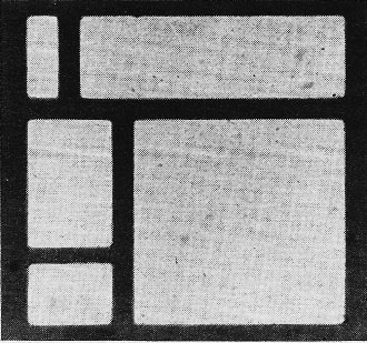
Fig. 3 - Integrated capacitors. The binary pattern here contains 5 capacitors of 1, 2, 4, 8 and 16 units of area.
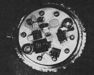
Fig. 4 - Hybrid integrated circuit. This one includes a multistage dc amplifier, with special, separate Rand C components, and is mounted in the same type of package that houses a completely integrated circuit.
How Are They Made?
Integrated circuits do not really represent a revolution in the state of the art. Rather, they are an evolution - the extension of manufacturing techniques used in transistor manufacture for over a decade. Like transistors, they have their beginning in crystal growing furnaces, like that in the cover picture, where from a melt of semiconductor material a tiny seed of silicon slowly emerges as a rod of single-crystal material. This material is relatively pure, but does contain a small number of deliberately introduced p-type impurities.
This crystal is then sliced into paper-thin wafers (approximately 1 inch in diameter and 0.006 inch thick). Each of these serves as a base, or substrate, for dozens or even hundreds of complete identical circuits, depending upon the complexity of the circuit structure and the values desired.
(Since the substrate represents a large portion of the total material employed for such circuits, obviously the material cost of a circuit borders on the negligible. The greatest single item of hardware cost in the entire circuit is that of the header, or package, in which the circuit "chip" will be eventually mounted to permit interconnection with other circuits in a more complex system. The cost of the integrated-circuit package is not appreciably greater than that of a conventional package housing a single, ordinary transistor. And, since the actual manufacture of a wafer of integrated circuits takes only one process step more than the fabrication of a transistor wafer, it is expected that, eventually, the cost of a complete integrated circuit should be little greater than that of a single transistor today.)
Actually, the basic wafer does little more than give mechanical rigidity to the integrated circuit. The parts themselves are all diffused into a microscopically thin n-type semiconductor layer epitaxially grown (Fig. 1) on top of the basic substrate.
The concept of integrated-circuit "parts" demands some explanation. An integrated-circuit resistor, for example, is merely a tiny area on the epitaxial layer which has been impregnated with a precisely controlled impurity of the opposite polarity (Fig. 2). The actual resistance of this area is determined by its dimensions as well as the resistivity of the semiconductor material diffused into the region. Typical resistance values range from about 10 to approximately 100,000 ohms.
Capacitors for integrated circuits (Fig. 3) are also made by diffusing one type of semiconductor material into an opposite polarity type. But, whereas resistors have two interconnecting points at opposite ends of the same material, one end of the capacitor may be the substrate itself; the other is the opposite-polarity material diffused into the substrate. Thus, a capacitor may be essentially an n-p or p-n junction which, in effect, is a junction diode.
There is very little difference between a diode and a diffused capacitor except in the way they are used. It is well known that any reverse-biased diode exhibits a capacitance effect. To use a diode as a capacitor, it is necessary only to keep it reverse-biased under all circuit operating conditions. Capacitance values available by this method depend upon the size of the diffused area. Practical values range from 1 to 1,000 pico-farads.
Transistors for integrated circuits can be made in the conventional manner. Transistors require three material layers, diodes and capacitors require two, and resistors only one. It should be obvious, therefore, that all diodes, capacitors and resistors can be made at the same time a transistor is manufactured.
Limitations
Progress made in integrated-circuit technology over the past couple of years has far outstripped even the most optimistic predictions. Yet everyone connected with the field will readily admit that this is just the beginning. True, a number of devices are in production and are actually being designed into equipment. But the scope of the art - the number of types of circuits being produced - is still limited.
Integrated-circuit production is largely confined to digital (switching) circuits for the computer industry. The reason is both technical and economic. Not only are digital circuits much simpler and less critical than linear (amplifier) circuits, the required parts and parts values for digital circuits are far more compatible with the present state of the integrated-circuit art.
For example, in today's technology, practical values of inductance with reasonably high Q's are still impractical in integrated circuitry. This automatically eliminates all forms of fully integrated tuned amplifiers. Moreover, capacitance values above 0.001 μf require too much space to be placed on a single chip with other "parts". Therefore, low-frequency amplifiers with R-C coupling and large bypasses cannot at present be made as fully integrated devices. And the number of parasitic parameters (stray inter component coupling) associated with integrated circuits is greater and more troublesome than in conventional wired circuits.
Hybrid Devices
All these factors can be and are being circumvented by hybrid devices: integrated circuits that can be combined with unencapsulated microminiature discrete components, all in the same package. Also, considerable study of unique circuit designs that may eliminate the need for inductances (R-C filters, etc.) and large capacitance values (active capacitance-multiplier circuits) is in progress. Results to date are, however, far from competitive with standard circuit elements.
Hybrid circuitry is a flexible technique for obtaining many of integrated-circuit advantages without being critically dependent on technological and economic factors. Sometimes called multiple-chip circuits, hybrid circuits consist of a number of silicon substrates, each containing one or more integrated-circuit parts. These chips are then mounted on a ceramic substrate and interconnected in a manner similar to conventional circuits.
Hybrid circuits are often combined with discrete microminiature inductors, crystal filters and other nonintegral parts. They are, therefore, highly versatile and, due to low design costs, can be adopted for custom-built and linear circuits in small quantities.
The flexibility of hybrid circuits is illustrated by a typical hybrid audio amplifier (Fig. 4). The individually mounted parts are interconnected either by separate wire bonds or by a metallization pattern. One "chip" contains a number of parts - in this case a Darlington-connected multistage de amplifier. For hybrid circuits, therefore, it is practical to make and stock a variety of commonly used "partial" integrated circuits and combine these with compatible parts to complete the final function.
Hybrid circuits can be mounted in the same packages as single-block integrated circuits, and are completely compatible. Since the design cycle for hybrid circuits is short, such devices can be used as an interim stage in the manufacture of integrated-circuit equipment. For example, early equipment models may be made with hybrid modules while fully integrated circuits are in the development stage. In subsequent models, fully integrated modules can replace the hybrid circuits on a 1-for-1 basis, without changing either the appearance or performance of the system.
New Circuit Design Principles
Integrated circuits mean a change in circuit design concepts. Just as transistors demanded a departure from vacuum-tube design principles, so integrated circuits require a new approach for best performance.
In conventional circuits, the active components (transistors and diodes) are normally far more expensive than passive ones (resistors, capacitors, etc.). With integrated circuits the opposite is often the case. In addition, an increase in the number of components to produce a given circuit function often results in little or no increase in cost. It may be convenient to use a greater number of stages to do a given job more reliably, rather than drive each stage to its maximum ratings.
The circuit designer, however, will be faced with the problem of which and how many stages and components are to be placed in a single integrated-circuit package. A particular "chip" size will hold only a certain number of components - often determined by component values. The designer may elect to place more than one chip in a package, thus reducing interconnection costs and increasing replacement cost. He may specify a larger "chip" to mount more components, but in doing so he reduces circuit yield and increases costs. He will have to circumvent inductors in his circuit design, and perhaps substitute active circuitry for large-value capacitors. He will have to design circuits within the limits of available integrated parts values and cannot rely on very close resistor and capacitor tolerances. Finally, he must be acquainted with the various parasitics in integrated-circuit fabrication and learn either to compensate for them or to use them in his circuit design.
But he will be starting on the ground floor. Today, the bulk of accumulated integrated-circuit knowledge is stored largely within the confines of semiconductor device manufacturers and those equipment companies who have set up close working relationships with the semiconductor concerns. For most working engineers, the design of integrated circuits requires a learning process similar to that involved in the changeover from tubes to transistors.
Although integrated circuits are being built in production quantities and are already designed into some equipment, even the most knowledgeable integrated-circuit engineer will admit that we have just scratched the surface of this new technology. But, if the progress made in the past year is any indication, acceptance of integrated circuits will be more rapid than that of any other major development in the history of this fast-moving industry.
This is the first of a series of articles on integrated circuits. The second will describe and explain the thin-film type of circuitry.
* Manager, Technical Information Center, Motorola Semiconductor Products.

Copyright: 1996 - 2026 |
About RF Cafe RF Cafe began life in 1996 as "RF Tools" in an AOL screen name web space totaling 2 MB. Its primary purpose was to provide me with ready access to commonly needed formulas and reference material while performing my work as an RF system and circuit design engineer. The World Wide Web (Internet) was largely an unknown entity at the time and bandwidth was a scarce commodity. Dial-up modems blazed along at 14.4 kbps while tying up your telephone line, and a lady's voice announced "You've Got Mail" when a new message arrived... |
Copyright 1996 - 2026 All trademarks, copyrights, patents, and other rights of ownership to images
and text used on the RF Cafe website are hereby acknowledge My Hobby Website: My Daughter's Website: |


