|
|||||||||||||
 |
|||||||||||||
Solid State Electronics - The Spacistor Et Al
|
|||||||||||||
Solid State columns: April 1967, August 1967, April 1966, August 1970, July 1971, October 1971, April 1972. Solid State
The "Time Gap" between the announcement of a new semiconductor development and its availability in commercial devices may be as short as 3 or 4 months or as long as 5 years. It depends not only on production problems, but on such economic factors as user demand and relative costs. Some developments never go beyond the laboratory stage.
Fig. 1 - With the correct bias and voltage applied to this new University of Michigan negative-resistance device, it acts like a unijunction transistor except that the V/I curve is much deeper. There are no practical applications for it at this time.
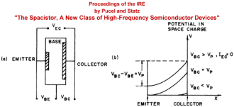
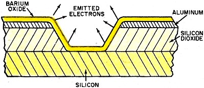
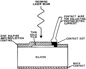
Fig. 2 - Developed at Stanford Research Institute, this semiconductor cold cathode supplies a source of electrons (similar to the cathode of a conventional vacuum tube) without heat generation. Quite some time ago, for example, one manufacturer announced the development of an intriguing device called a "double-base diode." Production versions were not sold until many months later, and then under a different name - the unijunction transistor! On the other hand, a very promising device, the "spacistor," has never been produced commercially and even its name has been forgotten - except by a few old-timers. It should be interesting to see what happens to several new laboratory developments. The Electrical Engineering Department of the University of Minnesota has announced the device illustrated in Fig. 1. It has a characteristic curve roughly similar to that of a unijunction transistor, but with a much deeper negative resistance dip. Unnamed as yet, the device consists of one n-type and two p-type contacts alloyed to a germanium bar. In operation, a reverse bias is applied to the middle p-type contact and a negative resistance characteristic is developed between the outer p-type contact and the common n-type terminal. An unusual semiconductor cold cathode for vacuum tubes is under development at the Stanford Research Institute. Dubbed a "transverse field semiconductor emitter," the cathode consists of alternate layers of metals, insulators, and semiconductor materials, subdivided into individual segments, as illustrated in Fig. 2. A pure silicon layer serves as one conductor, a silicon dioxide layer as an insulator, and a thin aluminum layer as the second conductor. The two conductors are bridged by a very thin (0.0001 inch) barium oxide semiconductor film. In operation, a voltage is applied to the two conductors. Current carriers (electrons) are accelerated in a stream from one conductor to the other through the semiconductor film, with some escaping and attracted to a nearby anode (or plate). A new type of photodetector - a metal semiconductor diode with an anti-reflection coating - has been developed at the Bell Telephone Laboratories. With a faster response time than pn or pin diodes, it is highly efficient, converting up to 70% of a light beam's photon energy into photoelectric current. The new photodiode's initial application will be in the detection of modulated light energy from a helium-neon laser. The device itself consists of a silicon substrate which is first coated with a semitransparent gold film, then with an anti-reflective coating of zinc sulfide, as illustrated in Fig. 3. A gold contact dot and wire near the edge of the metal film collect the photoelectric current created within the semiconductor's depletion layer, a region of high electric field adjacent to the metal film.
Fig. 3 - In this Bell Labs photodetector, the photons that pass through the gold film create electron-hole pairs at the gold-silicon junction. Current then flows through the external circuit connected between the contact dot and back contact.
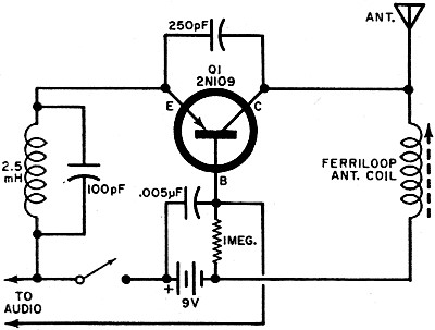
Fig. 4 - Modulation monitor devised by Bill Waddington can be used at any frequency if the coil is wound for that frequency. A simple amplified crystal set, it provides ample headphone volume. When light strikes the. coated metal sur-face of the new device, photons pass through it and create electron-hole pairs in the depletion layer. The released electrons and holes are immediately swept across the depletion layer to their respective contacts by the electric field, developing a current in the external circuit. The new photodetector, when fully perfected and in production, may make laser beam communication systems practicable for low-cost commercial, industrial, consumer, and hobbyist applications. Readers' Circuits. Needing a simple monitor to check the modulation of his 2-meter SCR-522 transmitter, reader Bill Waddington, WA7BCD (716 Clover Court, Cheney, Washington 99004), first tried an untuned diode detector arrangement. Not realizing enough headphone volume, Bill devised the simple, but sensitive, circuit illustrated in Fig. 4. If other coils are used, the design should be adequate for most amateur radio or CB monitoring applications. This circuit has a broadly tuned input coupled to the familiar diode with C1 serving as an r.f. bypass. The detected output signal is applied to a modified Darlington stage, Q1-Q2. On 2 meters, L1 is about 19 inches of #12 copper wire wound as a self-supporting coil. The transistors (Q1 and Q2) are pnp general-purpose units. Layout and wiring are not critical and the individual builder may follow his own inclinations as far as construction technique is concerned, using a breadboard, circuit board, or metal chassis base. Bill writes that he assembled his model in a small wood cylinder with the antenna and coil at one end, and the 'phone jack at the other end. The resulting "package" could be held conveniently in one hand. Another of those ever-popular "wireless microphone" circuits is illustrated in Fig. 5. This version was designed by reader Michael Mark (220 Forest Drive, Jericho, New York) who uses his model to broadcast music from his hi-fi system. Mike's circuit differs from the usual design in that he has used a modified common-base r.f. oscillator rather than the more familiar tickler-feedback, common-emitter configuration. The operating frequency is established by collector load Loopstick coil. Easily duplicated in the home workshop, this design requires relatively few components. Transistor Q1 can be a pnp type 2N109. The audio signal source may be a high impedance type microphone, a high lever output crystal or ceramic phono cartridge, or a modular audio amplifier with a 10 μF blocking capacitor. As with any AM broadcast band wireless microphone, the unit's output frequency should be adjusted for pick-up at a "dead spot" on a nearby receiver.
Fig. 5 - According to Mike Mark, this broadcast-band wireless mike has high enough modulation quality to broadcast music from his hi-fi system.
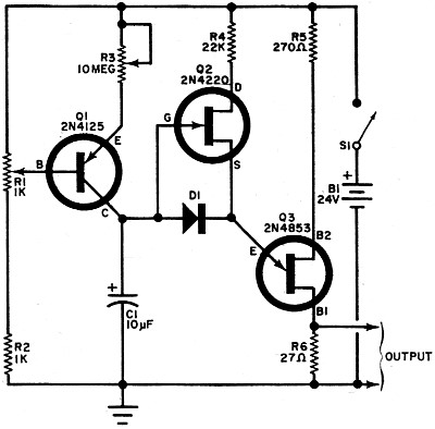
Fig. 6 - Time delays of up to 10 hours are possible with circuit suggested by Motorola if C1 and D1 are high-quality, low-leakage components. A glass-epoxy PC board should be used for best results. Manufacturer's Circuit. Timer circuits are legion. But ultra-long delay designs are few and far between. As a general rule, if a time delay of an hour or more is needed, common practice is to use a geared down motor fitted with a cam switch. Diagrammed in Fig. 6 is an all solid state design for delays up to 10 hours! Described in Motorola's "Semiconductor Newsbriefs" (published by Motorola Semiconductor Products Inc., P.O. Box 955, Phoenix, Arizona 85001), the circuit features a modified R-C arrangement as the basic timing mechanism, with the series resistive element replaced by a transistor-resistor (Q1-R3) network. This permits Q1 to act as a constant, very low current charging source for timing capacitor C1. In operation, C1 is charged slowly through R3 and the Q1 emitter-collector circuit. Base bias of Q1 is established by voltage divider R1 and R2, with both R1 and emitter load R3 serving to adjust the timing period. The FET Q2 is normally at cut-off and acts as an open circuit. As C1 is charged, a positive gate bias is applied to Q2, permitting the FET to conduct and apply a firing signal to the UJT Q3 emitter. Then Q3 switches from an open to a conducting state and develops an output signal pulse across base load resistor R6. Two components are somewhat critical, timing capacitor C1 and the biasing diode D1. High-quality, low-leakage units should be used here and the diode must be selected to have a leakage current of less than 10 μA. Leakage paths in the timing circuit must be avoided. If an etched circuit board is used for wiring, a glass-epoxy base is preferred over the more common paper-resin type. Product News. General Electric is now offering individual samples of their solid state light source, type SSL-1, for only $9.50 each. Emitting up to 40 footlamberts of visible light, the SSL-1 requires from 2 to 5 volts at approximately 50 mA. Details are available from General Electric Company, Miniature Lamp Department, P.O. Box 2422, Nela Park, Cleveland, Ohio 44112. A new line of moderately priced circuit breakers designed to protect transistors and rectifiers against thermal runaway damage is being offered by Astro Dynamics, Inc. (Burlington, Massachusetts 01803). Dubbed TRAN-Z-FUZE, the devices are of single unit construction and designed to be mounted underneath a transistor or rectifier in place of the usual insulating mica washer. In operation, heat is transferred by conduction from the semiconductor's body through the TRAN-Z-FUZE body to a set of self-contained, hermetically sealed, thermally operated contacts. These contacts open automatically as critical temperatures are reached and thus may be used to remove transistor power or to actuate an interlock relay. No technical details are available, but we've received word that Philips (Eindhoven, Holland) has developed a penlight-powered TV receiver measuring only 4 1/2" long by 1 1/8" in diameter. An earphone is used for listening to the audio portion of the program, with the earphone lead serving as an antenna! That's it for now - until next month, -Lou. |
|||||||||||||
|
|||||||||||||
|
|||||||||||||
 By Lou Garner, Semiconductor Editor
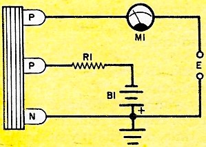


|
||||||||||||||||||||||||||||||||||||