|

Note: Ed Troy, owner of Aerospace
Consulting, LLC, was kind enough to offer a few of his articles for posting on RF Cafe. With more than 30 years
in the electronics communications design field, Ed has a lot of valuable knowledge to impart to us mortals ;-) This
fourth paper discusses the benefits of modeling and simulating an amplifier circuit as part of an effort to troubleshoot
an oscillating amplifier design. It comes to us in a timely manner after my recent
Notable Tech Quote highlighting
the often uttered "Amplifiers are oscillators that don't and oscillators are amplifiers that do" aphorism. The amazing
accuracy of modern high-end simulators makes such exercises useful for many types of troubleshooting efforts.
Using Simulation Tools to Debug an Oscillating Amplifier
By Ed Troy, Aerospace Consulting,
LLC
In this particular situation, I had designed an amplifier for a client based on a demo board from the manufacturer
of the semiconductor. The demo board worked as predicted by the manufacturer, and simulations of its performance
agreed well with measurements. However, when the client laid out the amplifier board and tested it, they complained
that it was not working properly and they were having problems. They could not identify the nature of the problems,
but I was pretty sure it was probably oscillating, or trying to oscillate. (Normally, I generally perform my own
layouts for clients, or at least guide them very carefully, which takes as much, or even more of my time than just
doing the layout, but this client insisted on doing the layout on their own without my close supervision. But, when
it did not work, they came to me to explain why my design did not work.)
So, the basic schematic is shown in figure 1. I am not showing actual values or part identifications for this
example.

Figure 1 - Amplifier circuit as designed By Ed Troy.

Figure 2 - Simulated amplifier performance.
However, when I measured the amplifier that was put together by the client on my network analyzer, the result
was very different and disturbing, as shown in figure 3. The measured board had a very strong gain peak at about
250 MHz, and the gain at 400 MHz was a few dB less than simulated. This indicates that it may be on the verge of
oscillating.
But, why would it oscillate? The simulation looked fine and the measured demo board looked fine, both on the
bench and in simulation. I suspected something in the layout and originally thought that I was going to have to
perform extensive electromagnetic simulation on the actual layout to identify the problem. (The board consisted
of much more than just this amplifier.) But, a quick review of the actual Gerber file used to generate the board
showed me something that looked very suspicious and typical of poor RF layout and the cause of many, many circuit
problems at these (and higher) frequencies.
Figure 4 clearly shows the problem, if you know what to look for.

Figure 3 - Measured performance of the amplifier as built.

Figure 4 - Layout of amplifier portion.
Notice the small circle to the right of the large pad in the lower left component. That component is the amplifier
transistor, and that circle represents a ground via. That is the only ground via for the transistor. And, to make
it worse, it is at the end of the center pin which is about as far from the bulk of the device, represented by the
large octagonal shape to the left of the center lead pad and ground via! Devices like this need multiple ground
vias, and they need them located not only where that one ground via is located, but a bunch should also be under
and around that ground pad. (Which is the bottom of the actual semiconductor device.) These ground pins are also
essential for heat sinking.
So, what we see in this layout is essentially a trace, consisting of the center lead pad and the short trace
to the ground via, from the device to the ground. The device, while electrically connected to ground, is connected
inductively to ground because of the distance between the actual ground via and the main device pad, which is under
the bulk of the device in that octagonal area.
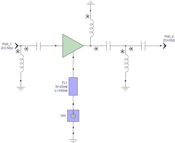
So, with that in mind, lets redo the schematic and add that trace in the ground path of the main device. This
results in the schematic shown in figure 5. Note in this case that I put in a short piece (100 mils long and 25
mils wide) of transmission line and a real via between the device ground and actual ground.

Figure 5 - Amplifier with inductive ground as in actual layout.
Figure 6 shows the simulated performance of this circuit with an inductive ground caused by inadequate grounding
of the power transistor along with the actual measured data from the board, as shown earlier. Clearly, you can see
that with this slight change, the simulated and measured performance is almost identical.

Figure 6 - Simulated inductive ground circuit with actual measured board data.
Fortunately, in this particular case, the transistor was located right next to the edge of the board. By soldering
copper foil to the ground tab of the transistor and wrapping it around the board and soldering it to the ground
on the bottom side of the board, a much better ground was achieved. To simulate this, the schematic in figure 7
was developed. Here, the 75 mil wide and 25 mil long trace was added to simulate the copper foil that was wrapped
around the board from the ground tab on the device to the bottom side. The bad, inductive ground is still there,
as it was on the actual board. But, now, the copper strap will help to lower the inductance between the device and
ground.

Figure 7 - Schematic of amplifier with wrap-around ground added.
Figure 8 shows the simulated data for the schematic in figure 7 and the measured data for the board with the
ground strap added. Clearly the oscillation tendency has been tamed and the conclusion that the problem was caused
by bad grounding in the layout was confirmed.
Again, this is another classic case showing not only the extreme importance of excellent grounding for all RF,
microwave, and wireless circuits, but it also shows the power of using simulation tools to troubleshoot design problems.

Figure 8 - Simulated and measured amplifier with ground strap added.
As an additional note, all of the simulated models for the capacitors and inductors were Modelithics (1) models.
These provide actual substrate and pad scalable models and thus make modeling much more accurate. Aerospace Consulting
LLC uses Modelithics models for all circuit modeling whenever possible.
1) Modelithics
To download an Adobe Acrobat copy of this paper,
click here.
Copyright 2015, Aerospace Consulting LLC. All rights reserved.
About Aerospace Consulting, LLC
Aerospace Consulting was started in 1982 as a part-time business. The founder,
Ed Troy, had
just changed jobs from working for a company that made telemetry transmitters and other military communications
equipment to a company that produced electronic article surveillance equipment. While working at ICI Americas, Ed
had an opportunity to do some design consulting with a company in New York that made hardware related to anti-submarine
warfare. Additionally, Narco Avionics needed help in redesigning some DME hardware because the transistor used in
their high power pulse transmitter was no longer available and a new amplifier had to be designed and developed.
With permission from ICI America's management, Ed started consulting on a part-time basis for these companies that
were clearly not competitors of ICI's EAS business. At the same time, Ed, a pilot with commercial, multi-engine,
and instrument ratings, was brokering aircraft in his free time. So, given the work for 2 aerospace-related companies
and the fact that he was brokering aircraft, Aerospace Consulting seemed a natural name for the company. Today,
it might seem a bit of a misnomer since most of Aerospace Consulting's customers are not aerospace companies
(although some are), but the name has not been changed. In the 25 years since going
full-time, Aerospace Consulting has grown dramatically both in terms of capabilities as well as the types of businesses
served. Aerospace Consulting also works with companies, both large and small, that have plenty of RF, microwave,
and wireless facilities and employees, but they just need some extra help to get through an especially busy time.
Posted March 25, 2015
|


