|
November 1965 Electronics World
 Table of Contents
Wax nostalgic about and learn from the history of early electronics. See articles
from
Electronics World, published May 1959
- December 1971. All copyrights hereby acknowledged.
|
My first exposure to bare
die integrated circuits was in the early 1980's, while working at the Westinghouse
Oceanic Division in Annapolis, Maryland. It was my first job as an electronics technician
after separating from the U.S. Air Force. After working there on the evening shift
for a couple years building sonar systems for the U.S. Navy, I had an opportunity
to move to the day shift if I could pass muster for a high level security clearance.
A small group of engineers, with just one technician, was formed to serve the needs
of a "special" customer. A couple other guys with more seniority them me interviewed
for the position, but they failed the background check, which included two polygraph
tests ...but I digress. Part of my job entailed building microcircuit assemblies
using bare IC die and surface mount passive devices epoxied to very tiny printed
circuit substrates, and then using a thermosonic wirebond machine to do the interconnections.
1 mil gold wire was used. A week-long class at the company's plant in Baltimore
provided the basics, but the work we did was very unique and required developing
new techniques that probably would not pass inspection by the crotchety Navy inspectors.
The image shown here of the 21-bit shift register is reminiscent of type die I worked
with. Most of the IC's I used were fairly simple logic gates (OR, AND, NOR, NAND,
Inverter, etc.) and some flip-flops (J-K, D, RS, etc.), mux/demux's, with an occasional
low-function microprocessor thrown in for good measure. We even had our own plastic
injection molding machine. I still think staring through a microscope for hours
on end is what made my formerly 20/15 eyesight so bad. I could tell you what we
did - and you'd love it - but then I'd have to kill you ;-) I honestly have never
told anyone, not even Melanie, what we did there. See also
Integrated Circuit Techniques,
The What and Why of Integrated Circuits,
Evolution in Electronics: Integrated Circuits,
Integrated Circuits: What's Available?, and
The Integrated-Circuit Industry.
Integrated Circuit Techniques
With an emphasis on recent developments in the technology, the
monolithic, isolated monolithic, the thin- and thick-film, MOS, and the hybrid techniques
are examined. Problems in going from discrete to integrated, examples, and testing
are included.
By Carl David Todd, Electronics Consultant
The already wide and yet expanding field of integrated circuits includes several
basic approaches for the fabrication of very small electronic circuits and a vast
multitude of combination techniques. Each has its own particular characteristics,
advantages, and limitations. Just as the various construction methods in building
houses are selected according to the end requirements and desires, so must the particular
fabrication process for integrated circuits be chosen according to the specific
needs and required characteristics.
Since no one integrated circuit technique yet developed can fully satisfy all
purposes and required specifications, it is well that we have several from which
to choose. In this article we will look at several possible methods for fabricating
integrated circuits and discuss their special characteristics with emphasis on their
features and limitations. Included will be the monolithic, isolated monolithic,
thin-film and thick-film, and MOS techniques with several possible combinations.
This article is directed to the engineer and technician who will be dealing with
the finished integrated circuit product either in equipment fabrication, checkout,
or repair and will attempt to answer the question "What can I expect of integrated
circuits?" Even though your present job has no direct connection with integrated
circuits right now, you will want to become familiar with them. It is very likely
that you will be seeing a lot of them in the near future.
The integrated-circuit techniques already developed have allowed a fantastic
degree of microminiaturization. Going back just a few years to the time before the
"semiconductor revolution," the accomplishment seems even greater. Who would have
thought that we could contain the circuit function of a dozen or more tubes with
associated resistors and capacitors within the size of this letter "O"?
Development of the integrated-circuit techniques has resulted not only in the
tremendous reduction of physical size, but has also produced great improvements
in the operating reliability of the over-all circuit through the reduction of connecting
wires and large, vibrating components.
Let's look at some of the common techniques for making integrated circuits and
see just what each method can offer and consider where each might run into trouble.
Monolithic Circuits
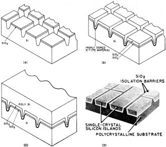
Fig. 1 - Isolated monolithic process. (A) Silicon "waffle" wafer
showing moats. (B) Oxide grown on moats of wafer. (C) Polycrystalline silicon grown
on wafer. (D) Final device.
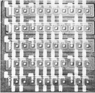
Fig. 2 - Diode matrix made with isolated monolithic process.
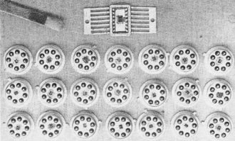
Fig. 3 - A 21-bit register (top) whose heart is a microscopic
wafer of silicon containing 110 transistors and 48 resistors, replaces 21 separate
microcircuits (shown here) in computers.
Monolithic means "single stone" and a monolithic circuit is one which is fabricated
within a single crystal of semiconductor material, usually silicon. The transistors,
diodes, resistors, and capacitors are all built right in the semiconductor material.
The bulk properties of the material along with the various characteristics of p-n
junctions me used.
The same basic processes for the fabrication of silicon transistors may be used
to make monolithic integrated circuits. The most common ones are the diffusion process,
the epitaxial process, or a combination of the two. The transistors, diodes, and
passive elements are made at the same time within the body of the silicon by diffusing
appropriate impurities through windows cut into an oxide coating by photo-chemical
etching.
The monolithic process has the greatest single capability of any of the processes.
It is possible to fabricate both active and passive components within a very small
volume and with all interconnections made by an aluminum evaporation that is etched
to provide the desired paths. The technique is basically that which has been successfully
used in the preparation of many transistors and hence is quite well developed.
One of the main limitations on the monolithic technique is the presence of distributed
diodes connecting the fabricated components to the silicon substrate material proper.
While it is possible to greatly reduce their effect by making sure that they are
always reverse-biased, we still have to contend with leakage currents which may
flow and with unwanted coupling capacitances which are present in any diode.
Another limitation on the monolithic process is the difficulty in obtaining proper
passive components. The range of the resistances which are practical is only about
20 to 20,000 ohms which places a severe restriction on the circuit designer. In
addition, the resistors even within the range of practicality have a rather large
temperature coefficient (approximately 0.7%/°C).
The capacitors are actually reversed-biased diodes and care must be taken to
make sure that they stay reverse-biased. Their value, which must be restricted to
rather small sizes, will be a function of the applied reverse voltage as is the
case with any semiconductor diode.
Still another limitation in producing monolithic circuits is the expense in making
the precision masks, several being required for each circuit. This restricts the
use of monolithic techniques to those applications where large quantities of the
same circuit are required. Even minor changes usually require scrapping the finished
integrated circuit and an masks. New masks must be made and the entire process repeated.
Isolated Monolithic Circuits
A variation of the monolithic process which overcomes many problems present with
standard monolithic techniques warrants separate consideration. In this approach,
portions of the original semiconductor block are isolated from each other either
by surrounding sides and bottoms with SiO2 (glass), a very good insulator.
Let's look at the basic process as currently being used by Radiation, Inc. The
process starts with a lapped and polished silicon wafer about 0.010 inch thick upon
whose surface a thin laver of SiO2 is formed by heating in an oxidizing
atmosphere. Moats or grooves are then etched around the areas which are to be isolated
by a normal photo-etching process to produce the results shown in Fig. 1A.
Very highly doped n- or p-type silicon is epitaxially deposited or grown within
the groove and then covered by SiO2, formed by heating again. The resulting
structure is shown in Fig. 1B. Polycrystalline material (not having a carefully
arranged lattice structure as the monocrystalline material required for transistors
and diodes) is then deposited over the entire surface. The grooves are filled and
the entire surface is covered with a thick coating, as shown in Fig. 1C.
The wafer is turned over and the original silicon wafer material is ground off
until the polycrystalline material is reached. The surface is then polished and
etched to leave small islands of the original silicon wafer from the polycrvstalline
material. These islands act merely as a structural agent, via a thin laver of SiO2,
as shown in the photograph of Fig. 1D. This photo does not show the heavily doped
n-region which is not always required.
Each of the isolated islands of silicon may then be treated as a separate chip
and processed in the same way as in the normal monolithic process. Very careful
control of the thickness of the wafer and the deposited coating is required. Let's
look at some of the features of this process.
Because of the glass isolation, we no longer have to make sure that we back-
or reverse-bias the isolation diodes and we have less than one-tenth the stray capacitances
present. Also, the leakage current between elements is greatly reduced, especially
if operated at high temperatures. Further, breakdown voltages of 1000 volts between
adjacent elements is practical. Another advantage of this technique is the possibility
of making both p-n-p and n-p-n transistors on the same substrate and the capability
of selective gold doping to achieve different characteristics for adjacent devices
on the same substrate.
A diode matrix, manufactured by Radiation, Inc. by the isolated monolithic technique,
is shown in the photograph of Fig. 2. The glass isolation region may be seen surrounding
each row of diodes in the matrix as well as the heavily doped n-regions. The n-regions
conveniently tie all of the cathodes of the diodes in a given row together.
This photograph also shows an interconnection means in which all diodes are connected
to the vertical interconnect buses and then disconnected by blowing out a portion
of the metallization. This is done by electrical discharge to remove those connectors
not needed in the matrix.
Thin-Film Circuits
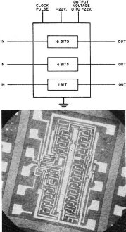
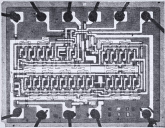
Fig. 4 - A 21-bit shift register. The functional block diagram
and a photomicrograph of the actual structure used.
Another technique which may be used to fabricate integrated circuits is the evaporation
and deposition (usually performed in a vacuum) of metals and dielectrics upon a
smooth surface, such as glass or vitrified ceramics. The usual method is to raise
the temperature of the material to be deposited above its boiling point in a vacuum.
The vapor is then allowed to condense upon the substrate through appropriate masks.
The resulting depositions are very thin and are measured in microns (millionths
of a meter).
Thin-film circuits have the advantage in that higher values of resistance are
possible and the temperature coefficient may be held to nearly zero if desired.
Because the resistance material is on the surface of the substrate, it is possible
to trim a given resistor physically to a precise value. This is achieved by making
it a little low in value to begin with and then carefully removing a small portion
of the material until the desired value is reached. It is also possible to control
the value of the resistance during deposition by monitoring it with a precision
bridge. The process is then stopped at an appropriate point and the resistance value
"frozen" at that level.
Capacitors made by the thin-film process are not voltage sensitive as is the
case with p-n junction capacitance. By careful alternation of metal and dielectric
deposition during the fabrication process, a multiple plate capacitor having substantial
capacitance is possible. Since the dielectric films must be very thin, breakdown
voltage can be a problem if even a very small defect occurs during the deposition
of the insulating material (usually silicon dioxide).
Since the deposition is generally made using a substrate of insulating material,
isolation between various parts of the circuit is much better than for the monolithic
technique. One of the greatest limitations to the use of the thin-film process in
its purest form is the lack of quality active devices. Although development transistors
and diodes have been made by this method, they have not been found suitable for
general use.
The thin-film circuit process has the same problem as the monolithic circuit
techniques regarding the requirement for precision masking. If a wide range of resistance
values is to be included within a given circuit, the number of masks required is
large and the actual number of process steps will almost always be greater than
for monolithic techniques. This is especially true if the circuit is complex.
Thick-Film Circuits
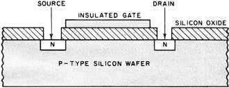
Fig. 5 - Cross-sectional view of an "n"-channel MOS device.
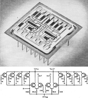
Fig. 6 - Photo and schematic of hybrid 4-input gate.
It is possible to fabricate circuits utilizing a thick-film technique in which
the interconnections and components are applied to a substrate by a silk-screen
process. This basic approach has been in use for many years with RC networks found
in radios, television sets, and hearing aids. The more recent development of the
Cermet materials (basically a combination of metal and glass) has improved the basic
capabilities of this technique considerably.
Interconnections used in the thick-film process are usually a silver-bearing
material and are fired at a rather high temperature. Temperature coefficients for
thick-film resistors are not as low as those obtainable with thin-films. Typically,
they are much better than those possible with monolithics.
Thick-film capacitors may be quite large in value since the dielectric to be
screened can have a large dielectric constant (300 to 500). Breakdown voltages can
be made as high as needed by increasing the thickness of the dielectric. This, however,
will decrease the capacitance.
No thick-film active devices are currently in use. We must therefore combine
thick-films with active devices made by an-other process, as discussed later in
this article.
MOS Technique
The metal-oxide-semiconductor (MOS - a field-effect device) process had been
applied to monolithic integrated circuits with notable success. Because the active
components on the chip are essentially insulated from each other, isolation gimmicks
are not required. The technique lends itself to low-cost, high-density digital integrated
circuits. These devices have a lower frequency response than other devices and consequently
clock rates for digital functions are limited to a few megacycles.
An example of the use of this new process is a 21-bit shift register developed
by General Instrument Corp. (Fig. 3). The silicon wafer measures 0.07 inch long
and 0.06 inch wide and contains 110 transistors and 48 resistors. Clock rate is
500 kc. and the unit replaces 21 separate microcircuits. Fig. 4 is a block diagram
and a photomicrograph of the circuit.
(Also refer to the cover illustration.) The register is actually three shift
registers in one package sharing a common supply and clock pulses. The three can
be used either independently or connected in series to give a total of 21 bits of
delay to an arbitrary data stream. By letting the output voltage be just a few volts,
it is possible to have the register drive other types of low-voltage n-p-n logic.
Fig 5 provides a cross-sectional view of an n-channel MOS. The two n-regions
labeled "source" and "drain" are diffused into the p-wafer by such methods as used
in the planar process (e.g., photo resist and oxide masking). The source and drain
are analogous to the cathode and plate of a vacuum tube, respectively. The third
element, the gate (analogous to the grid of a vacuum tube), is evaporated over the
silicon oxide between the two n-regions. The gate is insulated from the silicon
wafer and exhibits a resistance on the order of 1010 or more ohms.
In a type called the n-channel depletion MOS, drain current will flow even if
the drain-source (input) circuit is zero biased. For integrated digital circuits,
however, the n-channel enhancement MOS which exhibits zero drain current for zero
bias, is preferred. A significant characteristic of the enhancement type is its
low saturation voltage. This permits the design of simple direct-coupled transistor
logic (DCTL).
Hybrid Circuits
Each of the basic techniques described has limitations which might restrict their
use in many areas for one reason or another. However, each technique has certain
advantages. There are many possible combinations of portions of the basic techniques
which will result in an expansion of the capability of any of the single processes
with many of the desirable features retained. This approach leads to the hybrid
circuit.
One of the simplest forms of hybrid fabrication is the combination of several
"chips" or discrete monolithic blocks within a single package. This allows more
complicated circuitry to be fabricated than might be possible if the entire. circuit
were to be made as a single monolith. In some cases, it is either impossible or
at least impractical to make certain combinations of p-n-p and n-p-n transistors
on a single chip. For example, if matching is required for one reason or another,
it is much easier to perform the matching before assembly than to try to obtain
a perfect match with two devices on a single chip.
Isolation can be improved by the use of multiple chips and the circuit components
contained on each chip may be optimized independently. This becomes especially important
where it is necessary to include many active and passive components of different
types within a single circuit. Since the interconnections must be made by small
wires bonded to the individual connection terminals on each chip, assembly labor
can become relatively high. Each extra connection will also decrease the over-all
reliability of the device.
The multiple chip arrangement is also useful in developing prototype circuits
or configurations which are subject to change. It is possible to alter the design
of one chip without affecting any of the others and to add small discrete components
to the circuit.
Another hybrid form is the combination of thin-film passive components with monolithic
circuits. This is especially useful in the fabrication of circuits requiring large
resistances or low temperature coefficients. The monolithic portion is made in the
usual manner and then the thin-film portions of the circuit are deposited on top
of an insulation layer formed on the surface of the monolithic block. In a sense,
most monolithic circuits are in this category of hybrid because the final interconnection
is usually a thin-film deposition of aluminum.
Thick-films may also be combined with monolithic blocks in just about the same
manner as described for the thin-film combination. However, this is not as common.
A more usual combination of monolithic and thick-film circuits is the addition of
monolithic active devices or circuit chips to the substrate on which the thick-film
circuit has been screened. This combination allows all of the passive components
to be fabricated independently from the active components and can result in a very
workable arrangement.
An interesting hybrid combination is shown in the photograph of Fig. 6. This
particular circuit is for a four-input gate also shown in Fig. 6. The technique,
developed by Corning Glass Works, combines monolithic circuit chips with thin-film
resistors and thick-film interconnections and capacitors. The capacitors, if required,
are fabricated on top of the substrate first by silk screening a sandwich of gold
paste, niobate glass frit, another layer of gold paste, and finally a layer of protective
glass. A portion of each of the gold paste layers is left exposed to allow connection
to be made to the electrodes.
The substrate containing all the required capacitors, whose values may be controlled
by varying the physical area of the electrodes or the thickness of the dielectric
layer, is then placed in an oven and "fired" at a very high temperature. This permits
the binding of all layers together, devitrification of the glass dielectric, and
provides a hermetic seal over the finished capacitor. The dielectric constant of
the glass used for the dielectric is around 400 and the thickness may be a little
more than one-thousandth of an inch. This means that capacitance values up to 3000
pt. are practical.
If interconnection crossovers are required (or if they might greatly simplify
the circuit layout), they are easily made at the same time as the capacitors. When
the first layer of gold paste is screened, a small stripe of gold paste is placed
where the crossover is desired. During the screening of the sealing glass, the mid
portion of this crossover stripe is covered with a glass seal. This allows another
interconnection path to pass over the gold stripe without shorting and with very
little coupling capacitance. The dielectric constant of the sealing glass is only
around 5 or 6.
The substrate containing the capacitors and crossover stripes is then covered
with a thin film of tin oxide deposited without requiring a vacuum. The tin oxide
is etched away except where a resistor or interconnection line is required, employing
a photoresist technique. Places where a resistor is required are masked off by vinyl
silk screened on top of the tin oxide and the remaining area of tin oxide is plated
with copper, An electroless plating technique is used and copper is left only on
the exposed tin oxide.
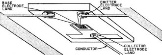
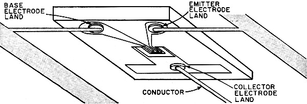
Fig. 7 - Construction of a transistor of the flip-chip form.
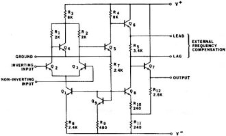
Fig. 8 - An example of an integrated operational amplifier.
Individual resistors may be trimmed to as close a tolerance as required (down
to 1/2%) by making the initial value a little too small and then sandblasting a
notch in a loop provided for that purpose. Several of these are visible in the picture.
Semiconductor devices of the "flip-chip" form are added to the tinned copper
interconnection. The flip-chip can be just a diode or transistor, or it might be
a complicated integrated circuit in monolithic form. Fig. 7 illustrates a "worm's-eye"
view of a single transistor as might be seen looking through the substrate.
This type of hybrid fabrication permits monolithic circuits of moderate complexity
to be combined with stable resistors. These resistors have a relatively low temperature
coefficient and are capable of being trimmed to close tolerances even after final
assembly. The fact that capacitors, having the characteristics of a hermetically
sealed ceramic unit, may also be included as a valuable asset.
Since the monolithic circuits may be broken down into functional sections, very
complicated circuit configurations are feasible with a minimum of interaction and
undesirable coupling. In addition, the availability of crossovers can greatly simplify
a layout design and decrease the distributed capacitances and inductances in high-speed
circuit interconnections.
Although the circuits as currently produced by Corning are enclosed in a hermetically
sealed package to protect the semi-conductor devices, it should be possible to adequately
protect them by normal passivation techniques or glass encasements. A mild conformal
coating would give added protection.
Converting to Integrateds
Let us consider the various factors involved in taking a circuit from an arrangement
using standard or full-size components and developing an integrated circuit which
will perform the same basic function. The difficulty and the over-all direction
taken would depend very greatly upon the actual circuit requirements.
Digital circuits are typically easier to integrate than analog functions since
any capacitors required are usually small in comparison with those which might be
required for an audio amplifier. Radio-frequency circuits often require coils and
transformers. While it is possible to fabricate a coil with a limited amount of
inductance by the thin-film technique, the range is very restricted and the "Q"
is very low. The large capacitor or coil problem is solved by means of adding on
miniature discrete components.
Let us assume that we must integrate a simple audio amplifier and study the design
decisions involved with the conversion from an arrangement using standard components.
A normal arrangement might use RC-coupled amplifier stages. Since the rather large
capacitors would be impossible to make in monolithic or thin-film form, we would
do well to consider a redesign to eliminate as many capacitors as possible and preferably
all of them. We may do this by careful design and by using a differential amplifier
or temperature compensation techniques to stabilize the bias conditions.
If a very minimum of size were required, we would perhaps best consider the monolithic
circuit process since it would be possible to contain the entire amplifier within
the volume of a TO-5 can or in a flat package roughly a quarter of an inch square
and 0.050" thick. To do this, however, we would have to eliminate all capacitors.
The circuit could be made of one monolithic block or it could be formed from several
monolithic chips within the single can.
Another approach might be preferable if the output power requirements were too
large for the monolithic technique; also, if the quantity were not sufficient to
warrant the fabrication of precision masks which might have to be modified several
times before the exact performance requirements could be met. In this case we would
best turn to the over-all hybrid approach using the flip-chip monolithic active
components with plated interconnections and thin-film tin oxide resistors.
The hybrid approach allows us to use standard chips for the matched pair differential
stage and other transistors with the custom-designed resistors and interconnections.
With this technique we have the advantage of circuit adjustment after fabrication
and can raise the value of certain critical resistors to insure proper balance or
setting of the bias point or gain.
Should an input isolation capacitor be necessary, we might consider the use of
a field-effect transistor (FET) for the input stage. The input impedance level would
then be high enough to allow the use of rather small coupling capacitors which may
be fabricated on the substrate. We could perhaps squeeze in a small miniature tantalum
capacitor attached to terminals provided on the substrate.
Some Examples
Examples of an integrated four-input gate and a shift register have already been
shown. Many digital circuits have been integrated in a monolithic form as might
be expected since certain forms of circuits are repeated many times within a given
piece of digital equipment. Also, the same type of circuit is more likely to appear
in different pieces of equipment of two different manufacturers.
Digital circuits can usually tolerate the rather coarse tolerances and limited
ranges for monolithic resistors. They may also be designed to operate over a wide
range of speed without any capacitors. A large number of companies offer monolithic
integrated flip-flops, gates, shift registers, and other digital circuits as standard
items.
Analog circuits are much more likely to be custom designed although common circuits
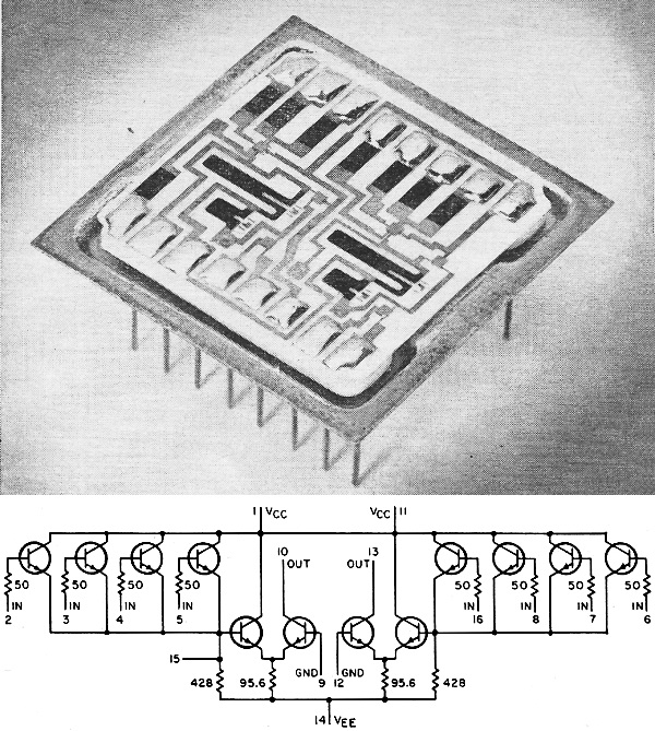
such as operational amplifiers are currently available as standard circuits. Fig.
8 shows the circuit diagram of one such amplifier (μA-702-A) offered by Fairchild
Semiconductor and yielding an open-loop voltage gain of several thousand and an
equivalent input drift due to temperature of about 5 μv./°C.
Radio-frequency amplifiers require tuned circuits and are, consequently, not
the easiest circuits to integrate. Nonetheless, some units have been built using
monolithic chips combined with discrete microminiature inductors. Motorola has developed
a 60-mc. amplifier with a 10-mc. bandwidth and an over-all gain of 61 db minimum.
Eight modules of four different types (input matching network, standard amplifier
stage, interstage tuning network and filter, and detector) are used and each is
contained within a 10-lead TO-5 can.
Testing Integrated Circuits
Testing of integrated circuits might at first seem practically impossible from
the service technician's viewpoint. He cannot get at any of the individual components
within a given module for replacement. Actually, if we consider any given integrated
circuit as a component with a given input and output requirement, the task becomes
more reasonable. Since we cannot repair the inside parts of an integrated circuit,
we need not concern ourselves with pinpointing the specific component which failed,
unless a critical failure analysis is necessary in order to provide direction for
a design change.
The integrated circuit is tested by applying the required bias levels, providing
the various input conditions, and monitoring the output to see if the specs are
satisfied. Since temperature effects may be the cause of some troubles, it will
generally be necessary to perform some testing at the extreme temperature conditions
to eliminate marginal circuits which might work perfectly well at room temperatures.
In the fabrication of integrated circuits, especially those of the monolithic
variety, the testing cost represents a sizable portion of the total. Many circuits
of the same type are usually made on a single wafer of semiconductor material. It
is necessary to test these individual circuits as soon as possible in order to prevent
any waste of labor on units which are defective. In some cases, it is only necessary
to do a rough check on the individual chip and then perform a more complete test
after the chip has been packaged.
Circuits using the hybrid thin-film, thick-film, and monolithic combination may
be modified by trimming their individual resistors. It may be wise to perform a
complete functional test on the circuit before the conformal coating is added. The
resistor adjustment can be made while the circuit is actually operating.
|