|
|||||||||||||
 |
|||||||||||||
Remedies for Poor Notes and Key Clicks
|
|||||||||||||
Although the application is a bit outdated, the lesson presented in this 1934 Radio News and Short-Wave magazine article about taming the chirps and thumps of keying Morse code via pulse shaping techniques is still useful today. While fully tamed (aka compensated / damped) commercial keys and keying circuits are available that require no technical knowledge of how they work or how to fine tune their operation, there are still many more older units operating that might need some tweaking. This is part 3 of a multi-issue article, so the few references to nonexistent illustrations are not typos. Figure 1 is reproduced from Part 1 of the article, and then the series picks up with Figure 7. Unfortunately, I have not yet acquired those previous two issues. Remedies for Poor Notes and Key Clicks - Part Three
Fig. 1 - Plate current during key clicks. Christ Kardas* The author shows the effectiveness of various key-filter circuits by means of oscillographs Key clicks and thumps are produced when suddenly applying a potential to a circuit which causes the current to build up immediately to a maximum value. They may also be produced when the circuit is opened if the current falls very quickly to zero. If inductance is inserted in the circuit, a time "lag" of the building up will result and eliminate or decrease this undesirable effect on closing the circuit. A combination of capacity and resistance will eliminate or bring to a minimum this interference quality when the key is being opened. Figure 1, Cases 1, 2 and 3, illustrate roughly some different possibilities.
Fig. 7 - Transmitter in the positive "lead" with only one choke in this same line, the "lag" effect was again produced.
Fig. 8 - Filter combination not very good.
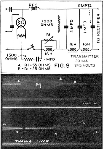
Fig. 9 - Effect of the "decay" with two different values of resistance shunting an inductance in series with the key.
Fig. 10 - Very good building up of the wave, but the key circuit resistance is too low and thus a long-drawn-out "decay" resulted. When no "lag" circuit is used upon closing the key, the current suddenly rises to its maximum value and quickly drops to zero when the key is released. This condition is represented in Case 1 of Figure 1. When suitable inductance is inserted in series with the key, upon opening and closing the circuit the "lag" effect is produced and Case 2 is the pictorial illustration. If it becomes necessary to suppress arcing between the key contact points by means of a condenser and a resistance in series and shunting the key or both the key and inductance, the arrangement will give an exponential decrease of current when the key is opened. This is also a time "lag" effect and is shown in Case 3. By placing a choke coil on each side of the key, a tapering effect at each end of the signal is produced as shown at g and m in Figure 2. In the wave, hg, the beginning shows a spurious oscillation, but this is due to the relay which did the keying. Its spring was not adjusted properly and therefore relay "chatter" resulted. The choke coil effect, however, can be seen from the line drawn at h, The "chatter" again appeared at cc, and by comparing it with that at the beginning of the signal hg, we see that both are alike. The dotted line b also shows effect of the choke coil. Note the constancy of the wave's amplitude and frequency at f. The "lag" effect at g is good, but it would be better if its duration were, say, about .008 second instead of .014 second. Figure 3 shows an oscillogram of a series of dots sent at a high rate of speed. Circuit conditions are a little different from those just discussed. That is, the resistance in series with the condenser shunting the key is now replaced by an inductance. Note in wave f the tapering effect produced at d, the end of the dot. The beginning is affected by relay "chatter" and also by a chirp. These dots were of very short duration and are shown to be about .02 second in length (not counting the time of building up and dying out). The relay "chatter." as represented by g and e, is lasting .005 second. It occurs about .004 second previous to the beginning of the signal. Waves A and B of Figure 4 show very nicely the effect of fair keying conditions, very good voltage regulation, and an excellent plate supply filter. The choke in the key circuit smooths out the power supply and also gives a time "lag" effect as may be seen by c and e. There is, however, a slight modulation at the beginning of the signal, but no chirp or key thump was present in the note. The effect at c (lower wave) appears because the oscillographic shutter opened and closed at this point. The end of signal which starts at g is not shown. Also the complete beginning of signal whose end is f is not shown. The choke in the keying circuit of Figure 4 was transferred to the left of the key and another oscillogram was made. This oscillogram is not shown for lack of space, but the negative showed a gradual building up - thus proving that the position of the choke actually makes a difference in the time "lag" effect. Figure 5 illustrates the bad effects one may get by using extra chokes, condensers and resistances indiscriminately. The key circuit as shown in the accompanying diagram has produced an unevenly modulated wave, as may be seen by looking at N. The note of the signal was "chirpy" with changeable frequency. At K and P there is a pronounced change of frequency more than that of the general drift shown throughout the wave. This can safely be blamed on the oscillator's instability. There is a possibility that the a.c. voltage feeding the transmitter was varying by a large amount. The interruption between g and f of wave m, also between j and k of wave N cannot definitely be accounted for; however. there is a possibility that the power feeding the transmitter was off for that .007 second. The circuit of Figure 6 is responsible for the long-drawn-out ends of the signals which are entirely too long. The beginnings of the dots build up nicely, but are a little too slow in reaching their maximum amplitude. A total of .012 second is consumed for the beginning of the dot and .03 second is used up for the decay, while the dot's maximum average amplitude consumes .043 second. Looking at M, it can be seen that the wave has a 60-cycle modulation; however, its frequency from the very beginning to the end of the decay is constant. This type of wave would not cause any chirps, key thumps or clicks, but it may cause the note to have a slight "swing." Keying the transmitter in the positive "lead" with only one choke in this same line, the "lag" effect was again produced as shown in the oscillogram of Figure 7. Wave C is that of a dot. The time "lag" is shown at d, which is affected by a change of frequency, thus causing a slight chirp at the end of the signal. Wave D is the same except that the key was held down a longer length of time and the film was turning at a much greater speed; thus spreading out of the wave resulted. As can be seen, its frequency is steady, but the lower part of this wave is somewhat modulated. No definite reason for this can be given. The filter combination of Figure 8 is not very good, as can be seen from the record of the wave. In wave B, the cut-off at c is much too long. If a smaller condenser were used, it would be shortened. The wave has a 40-cycle modulation which is undoubtedly due to causes at the receiving end and not at the transmitter. The waves on the second line were made as a continuation of the same signals (first line) , and these show hardly any modulation effects. They do show very much better building up, as at o, in comparison with the poor beginning a of wave B. It ought to be mentioned that there would be no chirp in either wave, but a slight key click will be heard. Figure 9 is a very interesting oscillogram, for it shows the effect of the "decay" with two different values of resistance shunting an inductance in series with the key. In wave M, the "decay" d is due to a 55-ohm resistance in shunt with the 16-henry choke coil while the "decay" z of lower wave is due to a 25-ohm resistance. The better of the two is, of course, that of wave M, and even this consumes too much time for the "decay." Figure 10 exhibits a very good building up of the wave, but the key circuit resistance is too low and thus a long-drawn-out "decay" resulted. *Owner and operator of short-wave amateur station W9FOK.
Posted June 22, 2023 |
|||||||||||||
 |
|||||||||||||
|
|||||||||||||


|
||||||||||||||||||||||||||||||||||||