December 1966 QST
 Table
of Contents Table
of Contents
Wax nostalgic about and learn from the history of early electronics. See articles
from
QST, published December 1915 - present (visit ARRL
for info). All copyrights hereby acknowledged.
|
This passive limiter is a simple combination
of cascaded "T" type resistive attenuators that are switched in and out of the circuit
based on the power level in the line. The design takes a bit of thinking due to
needing to retain a reasonable impedance match at the input and output throughout
various stages' conduction states. Arriving at an optimal value for resistors would
require a circuit simulator with a mathematically based optimizer, but, especially
for amateur radio work, close is good enough. That is not to say Hams are a bunch
of slackers - they're not - it's just that component and software resources are
not as readily available (aka "prohibitively expensive") for doing the analysis
and testing. In 1966 when this article was published, software did not even exist
for people without access to university or corporate computers. For most users these
days, it is cheaper to buy a limiter for 2- to 3-score dollars from suppliers like
Pasternack,
Mini-Circuits, and others. Note the distortion apparent in the
limited waveform.
A Passive RF Limiter
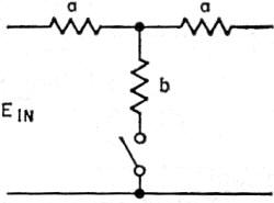
Fig. 1 - The basic limiter circuit. Closing S1
increases the attenuation without changing the frequency-transmission characteristics.
S1 should close when Ein reaches a predetermined value.
By George Schleicher.* W9NLT
An interesting audio limiter circuit using diode switching of resistive attenuators.
It does not "slice the top off the signal" sharply the way simple diode clippers
do, and thus has relatively little effect on the bandwidth of a speech signal.
A limiter circuit can be constructed with passive elements; the design of this
one is such that it will not generate high-order harmonics and it need not be frequency
sensitive in the audio range. The limiter uses a multiplicity of T-section attenuators
in tandem; each section is unusual in that a pair of diodes is connected in series
with the shunt arm. The diodes function like switches that open in the absence of
a potential but close when the voltage applied to any section of the attenuator
rises to a predetermined level. The closing of the shunt path causes the loss of
the attenuator section to increase to its design value. The switching action is
illustrated in Fig. 1.
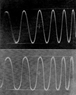
These scope pictures show the effect of limiting on waveform.
(A) Sine wave (765 cycles) before limiting; (B) Same signal after 8 db. of limiting.
As a result of the switching action each section of the attenuator will offer
a small loss to the low-amplitude portion of an electrical signal and a higher loss
to amplitudes of higher level. The maximum loss of any attenuator section is governed
by its design. The maximum amount of compression that the limiter can provide is
determined by loss of each attenuator section and the number of sections that are
connected in tandem. Good results have been obtained by using ten or twelve sections
in tandem, each section having a maximum loss of two or three decibels. The maximum
amount of compression that will be realized from a limiter of this type will be
equal to about half of the total loss of the attenuator sections.
When a voice signal is modified by limiting action there is necessarily a change
in the harmonic relationships within the signal. Listening tests indicate that heavy
limiting using a limiter of this type causes a voice signal to become somewhat "bassy,"
but this effect is hardly noticeable if the voice signal has been limited to a bandwidth
of only 3 kc. by means of a filter.
Diode Action
Solid-state diodes exhibit resistance in the forward conduction mode. This resistance
can vary from a fairly high value (over 10,000 ohms) to less than 100 ohms. It will
depend on the voltage across the diode and the materials of which the junction is
made. The materials also determine the manner in which the diode will begin conduction.
For example, copper-oxide junctions begin conduction more slowly than germanium
or silicon.
Design Principles
The characteristics of the diodes and the design of the attenuator sections should
be complementary. The diode resistance when conducting should be low enough to be
negligible in the shunt arm of the attenuator; in the nonconducting mode it should
be high enough to make the shunt appear as an open circuit. Pairs of diodes are
used so that the positive-going and the negative-going portions of a wave will be
similarly affected. The voltage at which the diodes begin conduction determines
the range over which the limiter will be effective. The limiter circuit should be
driven from a source having an impedance at least as high as the design impedance
of the attenuator sections, and it should be terminated in a similar impedance.
Since the diodes are connected in the shunt arm of the attenuator the basic limiter
design can be applied to both balanced and unbalanced (one side grounded) attenuators.
The circuit described here uses unbalanced T sections for simplicity.
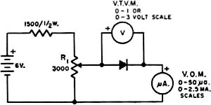
Fig. 2 - Test setup for measuring diode resistance. R1
is a linear control.
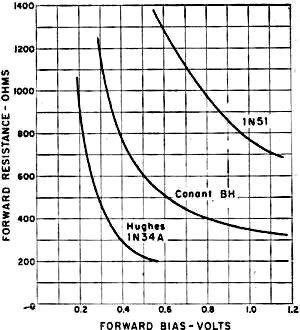
Fig. 3 - Resistance of three types of diodes measured with
the test circuit shown in Fig. 2.
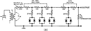
Fig. 4 - (B) Cascaded sections; note that the 75-ohm series
arm on the output side combines with the 75-ohm series arm on the input side to
make the single value of 150 ohms between adjacent shunt arms. Half-watt resistors
are satisfactory. In this circuit T1 is assumed to have a turns ratio
such that the plate resistance of the preceding amplifier tube is transformed to
a value of resistance that is low compared with the characteristic impedance, 600
ohms, of the attenuator. Likewise, the input impedance of the device to which the
limiter is connected is assumed to be high compared with 600 ohms. When this is
not true, R1 and R2 should be selected so that total input
and output impedances are 600 ohms.
A Practical Circuit
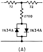
Fig. 4 - (A) Practical circuit for a single section.
Building a limiter of this kind can start with the acquisition of about two dozen
diodes of a given type. Their forward resistance should be measured using an arrangement
similar to that shown in Fig. 2. Measurements should be made in increments
of 0.05 or 0.1 volt starting at zero and continuing until the current through the
diode reaches its maximum rated value for the type of diode under test. A graph
can then be drawn plotting junction voltage against resistance (resistance is first
computed by dividing the voltage by the resultant current). Fig. 3 shows the
kind of curves that result when different diodes are measured this way. Using the
curve for the 1N34A as an example, it is evident that the resistance will drop to
about 200 ohms and that there is a "knee" in the curve at a potential of 0.45 volts.
The potential is significant because it corresponds to the input voltage at which
limiting action is maximized. The diode resistance at the knee (250 to 300 ohms)
is used in designing the attenuator sections.1 The shunt resistance used
in the attenuator should be about ten times the diode resistance at this point,
or 2700 ohms if the nearest standard resistor value is chosen.
Knowing that the shunt resistor will be 2700 ohms and desiring a loss of about
2 db. in the attenuator leads to the conclusion that the characteristic impedance
of the attenuator should be 72 ohms. (These conclusions are arrived at through the
help of the formulas given below.) The resulting limiter circuit is shown in Fig. 4.
It should be noted that between attenuator sections the output series resistor of
one section has been combined with input series resistor of the following section
(72 + 72 = 144 ohms). Again the nearest standard resistor value (150 ohms) has been
chosen for use in the circuit. The waveform photographs show how compression changes
the shape of a sine wave.
Appendix
Attenuators are lossy resistive networks. They are usually designed to have the
same impedance at their input and output terminals. Unbalanced attenuators are usually
referred to as "T" or "π" attenuators since these letters describe the circuit configuration.
Their balanced counterparts (for use in ungrounded circuits) are referred to as
"H" or "O" attenuator
Only four simple formulas are needed in designing T attenuators; they are as
follows:
Loss (expressed in db.) =
 {1} {1}
n =  {2} {2}
a (the series resistor value) =
 {3} {3}
b (the shunt resistor value) =
 {4} {4}
(Z is the characteristic impedance of the attenuator).
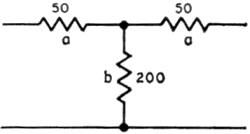
Fig. 5 - Attenuator used as an example for calculation as
described in the Appendix.
| 1 |
57.5 |
8500 |
| 2 |
115 |
4310 |
| 3 |
171 |
2840 |
| 4 |
224 |
2100 |
As an example of the use of these formulas, assume that you are designing an
attenuator of 150 ohms impedance with a loss of 6 db.:
6 =  {from 1} {from 1}
6/20 =  {from 1} {from 1}
0.3 =  {from 1} {from 1}
{antilogarithm of 0.3 = 2.0} from slide rule or log table
2.0 = 
 = 1/2 = n = 0.5
{solving for n} = 1/2 = n = 0.5
{solving for n}
a = 150  = 150 = 150
 = 50 ohms
{from 3} = 50 ohms
{from 3}
b = 150  = 150 (1/0.75) = 200
ohms {from 4} = 150 (1/0.75) = 200
ohms {from 4}
A single attenuator section of 150 ohms impedance and 6 db. loss is shown in
Fig. 5.
Some representative attenuator section values are shown below. They are included
as an aid in designing limiters of the kind described here.
These values are based on an attenuator impedance of 1000 ohms. For other impedances
the values should be increased or decreased proportionately.
1 The resistance measured in this way is a "d.c."
resistance, and while for higher accuracy in circuit design the dynamic resistance
should be determined, its measurement is considerably more difficult. The extra
complication would not be warranted unless it were necessary to know the exact attenuation
at different voltage levels.
|


 {1}
{1} {2}
{2} {3}
{3} {4}
{4}
 {from 1}
 = 150
= 150
 = 50 ohms
{from 3}
 = 150 (1/0.75) = 200
ohms {from 4}

