|
|||||||||||||
 |
|||||||||||||
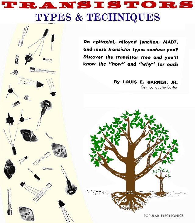
Transistors: Types & Techniques
|
|||||||||||||
Louis Garner was the semiconductor guru for Popular Electronics magazine in the 1960s when he wrote this article attempting to demystify the proliferation of over 2,000 transistor types. He devised a "transistor tree," tracing evolution from the obsolete point-contact transistor - unstable with high gain but noisy - to advanced designs balancing cost, frequency, power, and reliability. It covers pnp and npn basics, then details processes: grown-junction (inexpensive, good high-frequency); meltback diffused (similar, better response); alloyed-junction (popular for power); surface-barrier family (SB, SBDT, MA, MADT; excellent high-frequency, low voltage); post-alloy-diffused (PADT; thin base for speed); mesa (etched table-like structure, high-frequency power); epitaxial mesa/planar (optimized layers for voltage/frequency); and planar/epitaxial planar (diffused silicon, stable, passivated). Emerging field-effect transistors offer high impedance like vacuum tubes. Transistors: Types & Techniques
The transistor tree groups together similar types in branches. Field-effect transistors are the beginning of a new semiconductor tree. Do epitaxial, alloyed junction, MADT, and mesa transistor types confuse you? Discover the transistor tree and you'll know the "how" and "why" for each By Louis E. Garner, Jr. Since the invention of the transistor over a decade ago, manufacturers have been constantly seeking new methods to produce better and more reliable units - transistors that would not only have a broader range of operating capabilities, but also be lower priced. Often, a process has been developed which is capable of producing low-cost units. But, by its very nature, such a technique has resulted only in low-frequency (audio) types. Another process may deliver extremely high frequency units, or transistors with closely controlled characteristics, but be rather expensive. The net result has been a great variety of transistor types-over 2000 at last count-made by a dozen or more processes. Today, transistors are available with betas (gains) from 5 to over 50,000, power-handling capacities from milliwatts to hundreds of watts, and frequency capabilities from d.c. to thousands of megacycles. Prices, too, vary just as widely-from less than 50 cents to over $100 each, even in production quantities. PNP and NPN Except for specific electrical characteristics and maximum ratings, there are only two general types of triode transistors: pnp and npn units. These two classifications refer to the arrangement of the alternate layers of "p-type" and "n-type" semiconductor material making up the device. Whether the semiconductor material itself is basically germanium or silicon, the "p -type" material conducts by means of the migration of positive charges (called "holes"). Similarly, the "n-type" material conducts by means of the movement of negatively charged free electrons through the crystalline structure. The fact that many transistor manufacturers refer to their products primarily in terms of their internal construction has led to a good deal of confusion for newcomers to the electronics field (and, often, for "old-timers" as well). One firm will refer to its line of surface-barrier transistors. Another will sing praises about its high-quality mesa types. Still another will point out the advantages of its planar units. Sometimes, even minor refinements in production techniques will lead to new designations and such jawbreakers as VHF npn silicon epitaxial planar transistor. Such confusion, however, is really unnecessary - if you have some idea of what each basic type is all about. Let's look over the transistor tree and see if we can bring some order out of what may-for you-be chaos.
Point-Contact Transistor
Grown-Junction Transistor
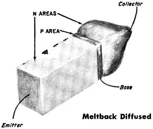
Meltback Diffused Transistor
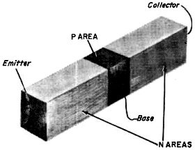
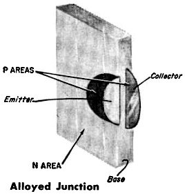
Alloyed-Junction Transistor
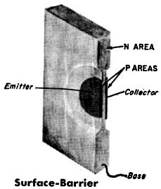
Surface-Barrier Transistor
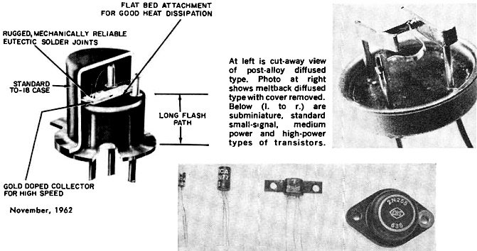
At left is cut-away view of post-alloy diffused type. Photo at right shows meltback diffused type with cover removed. Below (l to r) are subminiature, standard small-signal, medium power and high-power types of transistors.
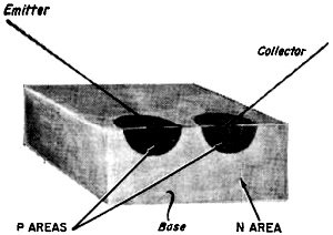
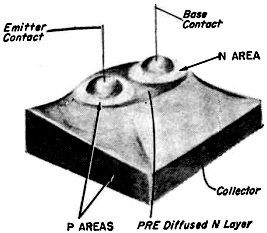
Post-Alloy-Diffused Transistor
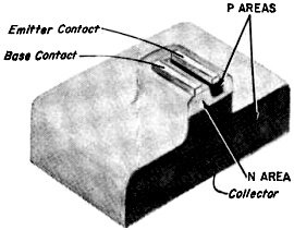
Mesa Transistor
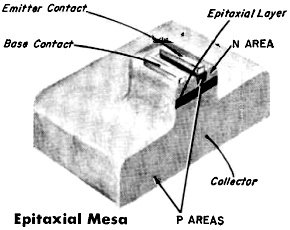
Epitaxial Mesa Transistor
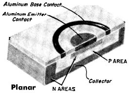
Planar Transistor
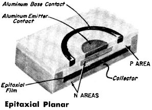
Epitaxial Planar Transistor
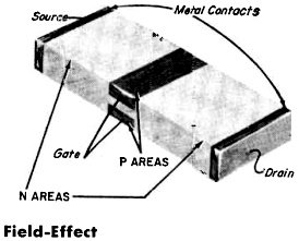
Field-Effect Transistor Point-Contact Although now considered obsolete, the point-contact type was the original transistor... the first, and for a while - the only, type produced. In its basic form, this type of transistor is made up of a small cube of n-type semiconductor material to which are attached two closely spaced fine metal wires or "cat's whiskers." The unit is treated during the manufacturing process so that atoms from the contact wires migrate into the semiconductor cube to form small p-type regions at their tips. One of the wires serves as the emitter electrode, the other as the collector, and the semiconductor cube is the transistor's base (hence the original name). Point-contact transistors have extremely high gain and good high-frequency characteristics, but they are also unstable, noisy, and difficult to manufacture. In addition, it is difficult to produce this type of transistor to close production tolerances, making the units quite expensive. Grown-Junction As the name implies, this type of transistor is made by "growing" the pn junctions during the original crystal-forming process. Two basic types have been produced. In one, the semiconductor material (germanium, for example) is "doped" with chemical impurity elements to give it both n- and p-type properties with, say, the n-type predominating. During the crystal-forming process, the growing rate is altered, changing the concentration of impurities so that alternate layers of p-type and n-type material are formed. A transistor cut from a crystal formed by this process is identified as a rate-grown type. (In a related manufacturing process, the concentration of impurity elements is changed by the addition of extra chemicals as the crystal is formed). Physically, grown-junction transistors are all quite similar in appearance and are essentially small rectangular bars of semiconductor material with alternating layers of n- and p-type material. Grown-junction transistors are relatively easy to manufacture and can be produced in large quantities inexpensively. In addition, they offer good high-frequency characteristics, low noise figures, and reasonably close tolerances. Meltback Diffused This type of transistor is manufactured from a small rectangular bar of semiconductor material similar in appearance to a rate-grown transistor. However, it is cut from a crystal containing both n- and p-type impurity elements, with the n-type predominating. One tip of the bar is melted into a drop and allowed to recrystallize. During the "refreezing" process, the p-type element concentrates at the junction between the melted and unmelted parts of the bar, forming a thin p-type base layer. The meltback transistor has general characteristics very similar to those of grown-junction units, but often with somewhat better high-frequency response. Alloyed Junction As this is written, the alloyed junction transistor is perhaps the most popular type. It is manufactured in both pnp and npn units and has a wide range of electrical characteristics. The majority of high-power (multi-watt) transistors are alloyed junction types. Again, the name gives a clue as to the manufacturing process, since the transistor is produced by alloying small pellets of metallic impurity elements to each side of a thin wafer of semiconductor material. If an n-type semiconductor is used, for example, the metallic pellets might be of indium. During the alloying process, the metal diffuses into the wafer, forming regions of the opposite type of semiconductor on either side. The wafer itself becomes the base, while the opposite regions become the emitter and collector electrodes. As a general rule, the collector is made larger than the emitter. Surface-Barrier Sometimes known as an SB type, the surface-barrier transistor is produced by an electrochemical process which permits the formation of a very thin base region. Typically, a wafer of n-type semiconductor material is placed between two very fine streams of a metallic electrolytic solution. A d.c. potential is applied, causing the solution to etch away the semiconductor material. When the desired thickness is obtained, the d.c. polarity is reversed, permitting the metallic solution to plate small metal dots on opposite sides of the etched-out region. These metal dots become the emitter and collector electrodes, while the etched-out wafer becomes the transistor's base. In some cases, the completed transistor is heated in an oven, permitting atoms from the plated-on metal dots to diffuse into the base wafer and forming a surface-barrier diffused type, or SBDT transistor. A modified, but related, etching technique is used to produce microalloy (MA) and microalloy diffused type (MADT) transistors. All transistors of the "surface-barrier" family, including SBDT, SB, MA, and MADT types, are characterized by their excellent high-frequency response, but limited voltage-handling capability. Post-Alloy Diffused This transistor, popularly known as a PADT type, is built up on a wafer of p-type semiconductor (typically, germanium). A pre-diffusion process gives a controlled depth of n-type material on the surface of the wafer. Later, two metallic pellets are placed near each other on the n-side of the wafer. One pellet, which eventually becomes the base electrode, contains only n-type impurity elements. The other contains both n- and p-type impurities and eventually becomes the emitter. The wafer itself becomes the collector. The assembly is heated under controlled conditions and the impurities in the base and emitter pellets diffuse into the semi-molten germanium. The n-type impurities are chosen to have a high rate of diffusion and penetrate deeply into the wafer to form an n-type layer. The p-type impurity in the emitter pellet diffuses slowly and to a limited depth. Upon cooling and recrystallization, the emitter pellet region is predominantly p-type material and is separated from the p-type collector by a diffused n-type layer which acts as the base. The resulting assembly is then etched and leads are attached. Mesa This type of transistor derives its name from its physical appearance rather than from the manufacturing process used. Under a powerful microscope, the mesa transistor looks something like the flat-topped hills or mesas which characterize the Southwest. The name, of course, is derived from the Spanish word for "table." The manufacturing process is a relatively simple one. A layer of, say, p-type semiconductor material serves as the collector. A thin film of n-type impurity is vapor-diffused on top of the p-type material to form the base region. Finally, the p-type emitter region is formed either by an alloying process or by vacuum evaporation techniques. An etching process is then used to produce the table-like structure which characterizes the mesa transistor. Mesa transistors are theoretically inexpensive to produce, and they have excellent high-frequency characteristics coupled with good power-handling capability. Epitaxial Mesa Physically, the epitaxial mesa transistor looks just like its "first cousin," the conventional mesa type. The difference between the two lies in the formation of a thin film between the diffused base region and the large p-type wafer which normally serves as the collector electrode. This film, known as an epitaxial layer because its crystalline structure is homogeneous with that of the main body collector, serves as an intermediate collector electrode. Even though it is the same basic p-type material, this film has electrical (resistivity) characteristics which are different from that of the main body collector, permitting the manufacturer to achieve an optimum compromise between breakdown voltage and high-frequency characteristics. Planar As might be suspected from its name, the planar transistor is formed on a relatively flat surface or "plane," made by diffusing the emitter as well as the base regions. In practice, a layer of, say, n-type semiconductor material (generally silicon) serves as the collector. An oxide film is formed on the top surface to act as a mask to prevent the diffusion of impurities into the material. Base and emitter regions are then formed by removing portions of the oxide film and diffusing suitable p- and n-type impurities into the collector. The base and emitter regions are formed in sequential steps, with oxidation and selective removal of oxide taking place prior to each diffusion step. Aluminum is deposited on both the base and emitter regions to provide low -resistance contacts. The final oxide film covers both junctions, preventing contamination and resulting in a passivated device with good electrical stability. Epitaxial Planar This type of transistor is virtually identical to the planar type, except for the addition of an epitaxial film, as discussed earlier. The manufacturing technique is similar to that used for conventional planars. Both conventional and epitaxial planar transistors couple superb high-frequency response with excellent electrical stability. Their basic characteristics are similar to those of mesa types, except for increased power handling capability and much lower leakage currents. Field-Effect A relatively new type, the field-effect device is a "transistor" only by definition, since its construction and operating principles are different from those of more familiar units. Even its electrodes have different names, being identified as source, gate, and drain, rather than as emitter, base, and collector. It has an extremely high input impedance (in the megohm range) and behaves somewhat like a low-voltage vacuum tube. A typical field-effect transistor consists of a bar of, say, n-type semiconductor material (such as silicon) which has had p-type impurities introduced into opposite sides, creating pn junctions and forming an n-type channel between the two p-type regions. Metallic contacts are made at opposite ends of the bar to serve as the source and drain electrodes, while the p-type regions become the control electrode or gate. In practice, the application of a reverse bias to the gate develops an internal electrical field which limits the current flow between the source and drain electrodes. Since the gate is reverse-biased, it presents a high input impedance to an external signal source. As this is written, the field-effect transistor is still considered a developmental device. If it becomes popular, there is a good chance that a variety of construction methods will be developed for it, just as they have for more familiar transistors. |
|||||||||||||
 |
|||||||||||||
|
|||||||||||||

|
||||||||||||||||||||||||||||||||||||