|
January 1955 Popular Electronics
 Table of Contents Table of Contents
Wax nostalgic about and learn from the history of early electronics. See articles
from
Popular Electronics,
published October 1954 - April 1985. All copyrights are hereby acknowledged.
|
Shortly before Christmas,
1947, the experimental work of Bell Laboratories scientists John Bardeen, Walter
Brattain, and William Shockley resulted in the world's first semiconductor transistor.
With proper biasing, the germanium transistor demonstrated an ability to produce
signal gain. The signal fed to the base resulted in a higher amplitude signal at
the collector. Voila, the device which would ultimately replace the vacuum electron
tube had been invented. The rest, as they say, is history. Aside from a few high
power applications, the only new equipment produced that uses vacuum tubes are retro
things like audio amplifiers and simple receivers. Of course, there is still a large
cadre of vacuum tube users in the Amateur Radio real and vintage equipment restorers.
If you have never watched a chassis full of tubes turn on and begin glowing, it
is worth your while to find someone with an old radio - or even a TV - and take
in the nostalgia.
Meet the Transistor

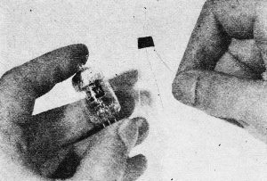
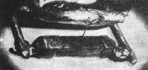
Fig. 1 - Miniature vacuum lube dwarfs the transistor which
can replace it. Later models are even tinier.
A tiny component that will revolutionize the entire electronics industry
- can operate from dry cells.
Few electronic inventions have captured the public's interest as has the development
of the transistor. This device, although requiring but 1/1000th the power and a
small fraction of the space of a vacuum tube, may be used as an amplifier, detector,
or oscillator and is thus capable of handling many of the jobs that vacuum tubes
are normally employed to do. In addition, since the transistor has no filament to
burn out and because it operates at comparatively low temperatures, it has a life
expectancy from 10 to 20 times greater than the average tube.
For these reasons and because of its small size (see Fig. 1) it has virtually
replaced tubes in the manufacture of hearing aids. It is also being used in military
equipment, specialized communications gear, and in certain types of instruments.
Eventually it will be used in portable receivers, home radio and TV sets, and auto
receivers. Tiny transistorized "wristwatch" and pocket-sized transmitters and receivers
have already been built experimentally and offer commercial possibilities.

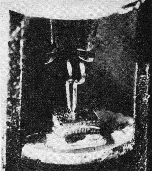
Fig. 2 - A cutaway view of a point-contact transistor. Note
two "cat's whiskers".

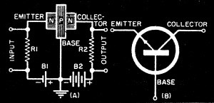
Fig. 3 - (A) Basic transistor amplifier. (B) Symbol for
an "n-p-n" junction transistor.


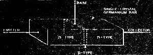
Fig. 4 - Diagram and photo of an "n-p-n" junction transistor.
Note changes from Fig. 2.
Transistors are made possible by the electrical properties of a group of materials
known as semi-conductors, consisting of substances which may act either as conductors
or insulators, depending on their physical conditions. Germanium, silicon, and selenium
are the most popular semi-conductors, with germanium being used almost exclusively
in the manufacture of transistors.
In a normal conductor, such as copper or silver, current flows when an electrical
voltage is applied to the material causing a movement of free electrons through
the substance. In a semi conductor, the application of voltage alone may not be
sufficient to initiate current flow - some other physical condition may be necessary
such as the presence of light, heat, or of an additional electrical field. The current
flow, when it does take place, may consist not only of the movement of free electrons
but may also include the movement of electrical "holes" through the material.
A "hole" is formed when an individual molecule loses an electron. The molecule
lacking an electron may pick up one from a nearby, electrically neutral molecule,
thus leaving the second molecule with a hole and a net positive charge. In this
way, the hole may travel through the substance, jumping from molecule to molecule
and producing a current flow which acts just as if it consisted of movement of positively
charged particles.
Although current flow through a particular substance may consist of a movement
of both holes and electrons, if the current flow is made up primarily of a movement
of holes, the material is called a "positive-carrier" or p-type semi-conductor.
If the current flow is made up primarily of a movement of electrons, it is called
a "negative-carrier" or n-type semi-conductor. A transistor is made up of a combination
of these materials.
Types of Transistors
Transistors are usually divided into two basic types, depending on their method
of construction, i.e., the point-contact and the junction types. A cutaway view
of a point-contact type is shown in Fig. 2 while a junction type is illustrated
in Fig. 4.
A point-contact transistor consists of a small cube of semi-conductor material
with two fine wires or "cat's whiskers" contacting its surface. Electrical connections
are made to the semi-conductor, called the "base", and to each of the two contact
wires - one of which is called the "emitter", the other the "collector". If n-type
semi-conductor material is used, it is called an n-base point-contact transistor.
Small p-type areas are formed under the contact wires during manufacture. If p-type
material is used in the base, the transistor is a p-base unit, and small n-type
areas are formed under the tips of the contacts.
A junction transistor consists of a "sandwich" of two types of semi-conductor
material, with the inner layer of different material from the two outer layers.
The basic construction is shown in Fig. 4. If the inner layer is of p-type
material, the unit is called an n-p-n junction transistor - if of n-type material,
a p-n-p transistor results. The n-p-n type is shown in Fig. 4. Electrical connections
are made to the two outer layers and to the inner layer of the "sandwich", with
terminals identified as "emitter", "base", and "collector", just as in the case
of the point-contact type.
How Transistors Work
Operation of the transistor may be understood by referring to a basic transistor
amplifier circuit (see Fig. 3A). An n-p-n junction transistor is used.
In operation, the emitter-base circuit is "biased" by battery B1 in
such a way that a low resistance is offered to the flow of current through the n-p
emitter-base junction. The collector-base circuit, on the other hand, is biased
with reverse polarity by battery B2 and offers a high resistance to the
flow of current, in fact, current flow can only take place through the p-n base
collector junction because of the excess of electrons produced by the current flow
in the emitter-base circuit.
If a signal is applied to the input terminals (across R1) the variations
in the emitter-base current which result will cause a variation in the number of
free electrons in the base, with resulting changes appearing as an amplified signal
across R2. In practice, the emitter and collector currents may be on
the same order of magnitude, but a considerable signal power gain is obtained since
the collector circuit represents a high impedance while the input (emitter-base)
circuit represents a low impedance.
Operation of a p-n-p transistor amplifier is similar except that conduction in
the base-collector circuit is principally by means of "holes" instead of electrons.
The schematic symbol used to identify an n-p-n type transistor in wiring diagrams
is shown in Fig. 3B. The base is represented by a straight line, with the emitter
and collector terminals identified by slanting lines to the base with the emitter
further identified by an arrowhead pointing away from the base.
The p-n-p type transistor is wired directly opposite from the n-p-n type, that
is, the collector voltage is negative while the emitter voltage is positive. The
symbol for the p-n-p type is identical to that for the n-p-n except that the arrowhead
points toward the base instead of away from it.
In this article we have discussed the basic principles of transistors and explained
how they can be used in a simple amplifier. Subsequent issues will describe other
amplifiers as well as detectors and oscillator circuits using transistors. END
Posted August 20, 2019
(updated from original
post on 10/7/2011)
|


