|
|||||||||||||
 |
|||||||||||||
Karnaugh Maps for Fast Digital Design
|
|||||||||||||
With the high degree of computer automation at this point in time, it is doubtful that many people still bother to perform digital logic simplification manually by using a Karnaugh Map. Online apps like this one (KarnaughMapSolver.com) do all the heavy lifting for you, producing minterms, maxterms, a truth table, and a written-out Boolean expression. Back in the late 1980s when I was working on my BSEE at UVM, the Karnaugh Map, created by Maurice Karnaugh, of Bell Labs, was introduced in a digital electronics course. It was a fairly easy concept to grasp. Is it taught in electronics curricula these days? This 1975 Popular Electronics magazine article provides a great introduction to the Karnaugh Map. It appeared during the era where large scale integrated (LSI) microcircuits were being widely designed into all forms of electronic products. Karnaugh Maps for Fast Digital Design
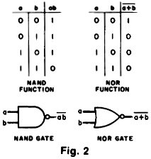
Have you ever tackled a digital design project with vim and vigor-only to find yourself entangled in a morass of logic ones and zeros and a "this goes up, and that goes down" nightmare? If you have, don't despair. There is a much neater, much simpler method than the brute force approach. This article provides a coherent approach to digital design. The method Is not a substitute for intuition and practical seat-of- the-pants experimentation, but a tool for getting the end results quickly. Before getting down to actual techniques, it might be wise to do a little reviewing. The truth tables for the AND, OR, and NOT (or COMPLEMENT, or INVERTER) functions are shown in Fig. 1. The function a AND b is written ab; a OR b is written a + b; and NOT a is written a. Note that + as defined here is different from ordinary addition, and merely symbolizes the function defined by the truth table of Fig. 1. A truth table is simply an array, one side of which contains all possible combinations of the input variables and the other side of which contains the corresponding values of a logic function or output. Figure 1 also shows the digital logic gate symbols for the three functions.
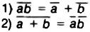
In manipulating the basic functions to form more complex ones, it is expedient to have available two important, yet simple, rules of basic logic theory known as DeMorgan's Laws. Figure 3 contains truth tables for the logic functions ab, a + b, a + b, and a-b. Comparing them yields the formulas of DeMorgan's Laws:
These formulas are useful in implementing digital functions using only NAND or only NOR gates. Why Map Techniques?
Suppose we are faced with designing the digital black box of Fig. 4, which has three inputs a, b and c, and a single output f(a,b,c). The black box is to provide a logic one output under the following input conditions: a=b=c=1, a=c=1 and b=0, a=0 and b=c=1, or a=b=0 and c=1. How can we manufacture the digital logic inside the box from this specification? One possible answer is to be methodical. A person unfamiliar with map techniques - but very methodical - might reason in the following way. "The output function f(a,b,c) is logic one whenever a=b=c=1. An AND gate puts out a one whenever all inputs are logic one, so let's use an AND. But the AND output is zero for all other input combinations, and f(a,b,c) is a one for several other input conditions. "Well, the AND gate did pretty well for the first input combination, so why not try it for the second? Let's take the complement of b by passing it through an INVERTER and run it into an AND gate with a and c. This AND will put out a one when a=c=1 and b=0, as desired. This seems to be working well, so let's do the same with each of the other two combinations."
Now this logic design works. It will do the digital job, but it is inefficient. It requires four AND gates, one OR, and two INVERTERs. This is costly, and it would cause quite a few layout problems because of the numerous interconnections. In addition, the design procedure outlined above is slow and, for more complicated circuits, error prone. What can be done to 'streamline the procedure? The answer is the Karnaugh map. This is just a rectangle divided up into a number of squares, each square corresponding to a given input combination. The Karnaugh map of our function f(a,b,c) is shown in Fig. 6. The right half of the map corresponds to a=1, the left half to a=0 (a=1), the middle half to b=1, and so on. The basic idea is that there is one square for each input combination. If we write into that square the value of the output function for that particular input combination, we will have completely specified the function. The ones and zeros in Fig. 6 are the values which f(a,b,c) assumes for the associated input variable combinations.
Using a Karnaugh Map
Using the three-variable map as an example, note that there is one box for abc, one for abc, another for abc, and so on, with abc corresponding to the input combination a=1, b=1, c=1; abc to a=1, b=0, c=1; and abc to a =0, b =1, c =0; etc. Each box, then, corresponds to a single row in the truth table. The map is arranged in such a way that half of it corresponds to the uncomplemented form of a given variable and the other half to its complemented form; and the variables are interleaved so that every input combination corresponds to exactly one square, and conversely. Usually only the uncomplemented form of each variable is written - it being clear that the other hall of the map corresponds to the complemented form.
The logic function in Fig. 9 is not at all simple looking. The question is, how can the function be reduced to its simplest form? Variables can be eliminated from the function by use of the following definition and rules: Definition: Two boxes are adjacent if the corresponding variables differ in only one place, for example if one box corresponds to a b c and the other to abc. Notice that boxes on opposite edges of the map are adjacent under this definition. Rule 1: If two boxes containing ones are adjacent, the single variable which differs between the two (uncomplemented for one, complemented for the other) can be eliminated and the two boxes combined. These two boxes correspond to the AND function of all the variables except the one eliminated. Rule 2: If four boxes containing ones are adjacent in such a way that each box is adjacent to at least two others, these boxes can be combined and the two variables eliminated-those two which appear in both complemented and uncomplemented form somewhere within the group. The group of four corresponds to the AND function of all the variables except for the two which have been eliminated.
Rule 4: The various AND functions produced by the above groupings are "ORed" together to yield the simplest function. It should be noted that a given box can be included in more than one grouping if that will simplify the overall function, but each grouping should contain at least one box which doesn't belong to an existing grouping (otherwise, this would lead to redundancy).
BCD-to-Decimal Decoder Consider the BCD counter of Fig. 11, with the four output variables a, b, c, and d. Suppose we need to decode the count of decimal eight and provide a control pulse, lasting one clock period, to some other digital circuit. We must build a logic function defined by the truth table of Fig. 11. This truth table introduces a new variable, called a don't care and given the symbol "X" The don't care means that we can define the output function f to be either zero or one for that particular input combination-simply because the input combination will never occur. A BCD counter never counts above decimal nine. The X's can be given values of zero or one so as to simplify the resulting function. In our case, the don't cares have been chosen as indicated by the smaller ones and zeros on the map. Notice the very simple form for the function f8, which can be constructed from a single AND gate and an INVERTER. The preceding was an example of what is called combinational logic. The outputs at a given time are dependent only upon the inputs at that time. Actually, the gates used to build up a logic function have some delay. In the case of combinational logic, though, this just means that after the input values are established, there is some flat delay before the output value is established. The delay is critical only if we have to compare the output value with another being similarly generated. If this is the case, we could encounter problems with the timing margins.
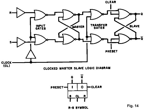
If the inputs have been in one state for a long time, the circuit will have settled into a stable situation with q1, q2, and q3 identical with Q1, Q2, and Q3, respectively. Now suppose one or more of the inputs changes values. Then no longer will the small q's be the same as the upper-case Q's. After the passage of (delta) time corresponding to the gate delays, though, the values of Q will have propagated through to the outputs, and the small q's will again be identical with the large ones. For a given set of input values, then, the small q's are called the unstable states and the large ones the stable states of the sequential machine. The feature which allows memory storage and other effects is the regenerative characteristics created by the feedback. The R-S Flip-Flop An R-S flip-flop is a one-bit digital memory whose output is set to the one state by a one on an input set (S) line and to the zero state by a one on another line, called the reset (R). An incomplete truth table for this device is sketched in Fig. 13. It is incomplete because the output stable state is specified not only in terms of ones, zeros, and don't cares, but depends in addition on the present (unstable) state q. We can form a complete truth table by including q as one of the input variables, thus creating a feedback situation. The complete truth table is also shown in Fig. 13, along with the resulting Karnaugh map and the derived logic equation for the state Q. Note that we must always have RS=0 (called the RS flip-flop constraint) to keep from violating the condition that R=S=1 must never occur. Figure 13 also shows how DeMorgan's Law is used to get the function into a form requiring only NOR gates for its construction. By assuming all three possible combinations of input variables (remembering the R=S=1 is disallowed from ever occurring) and computing outputs, the truth table can easily be verified. It is also easy to show in this way that the output labeled Q is, indeed, the complement of the output labeled Q for all input conditions except the disallowed R=S=1. The Clocked R-S Master-Slave Flip-Flop
This type of sequential machine is depicted in Fig. 14. When the clock goes high, the R and S inputs are passed through the input gates and stored in the master. When the clock goes low, the input gates are disabled, and the information is coupled through the transfer gates into the slave flip-flop. The function of the preset and clear inputs is evident. Try assuming a set of input values for R and S, and trace the information flow, letting the clock change as described above, to convince yourself that the unit performs the R-S function. The J-K Flip-Flop
Let's use the clocked R-S flip-flop to build the J-K from our derived equation. For this purpose, let S=JQn and R=KQn be the inputs to the clocked R-S. According to the R-S equation, Qn+1 = S + RQn = JQn + (KQn)Qn Now, applying DeMorgan's law to KQn, we get Qn+1 = JQn + (K + Qn)Qn = JQn + KQn + QnQn. But QnQn = 0 always, so Qn+1 = JQn + KQn which is the J-K flip-flop equation. Notice that the R-S constraint is satisfied, since RS = (JQn)(KQn) = JK(QnQn) = 0 Fig. 16 shows the construction of the J-K from the R-S using two AND gates. Again, test the operation by assuming a set of conditions for J and K and tracing the logic flow. A glance back at the incomplete truth table will reveal that if J=K=1 (J and K inputs tied to a logic one) the J-K forms a toggle flip-flop. The preceding examples have been intended to accomplish two things. In the first place, knowledge of the logical operation of the various types of flip-flops is essential in order to use them intelligently in an original design. As a second objective, they have provided an effective demonstration of the economy of thought which results when the Karnaugh may is used in a digital design effort. |
|||||||||||||
 |
|||||||||||||
|
|||||||||||||
 By Art Davis
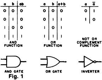
 A truth table is one way of specifying a logic function - the Karnaugh map
(pronounced Kar-no) is another. To get an idea of what such a map is, and why it
is a convenient tool, let's look at a practical digital design problem.
A truth table is one way of specifying a logic function - the Karnaugh map
(pronounced Kar-no) is another. To get an idea of what such a map is, and why it
is a convenient tool, let's look at a practical digital design problem. 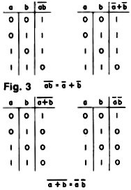 With all the AND gates and INVERTERs arranged as above, our methodical
experimenter will then observe that, since f(a,b,c) is to be a logic one
whenever the input variables form the first combination, or the second, or the
third, or the fourth, all he has to do is OR the outputs of the four ANDs to
generate f(a,b,c). The resulting logic is shown in Fig. 5.
With all the AND gates and INVERTERs arranged as above, our methodical
experimenter will then observe that, since f(a,b,c) is to be a logic one
whenever the input variables form the first combination, or the second, or the
third, or the fourth, all he has to do is OR the outputs of the four ANDs to
generate f(a,b,c). The resulting logic is shown in Fig. 5.  Now recalling our methodical design procedure, it is easy to see that each
square which has a one in it corresponds to the AND function of those input
variables, and f(a,b,c) can be generated as the OR function of all of the ANDs.
Now recalling our methodical design procedure, it is easy to see that each
square which has a one in it corresponds to the AND function of those input
variables, and f(a,b,c) can be generated as the OR function of all of the ANDs. 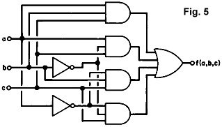 A key factor arises here. It isn't necessary to include all of these AND
functions, and the Karnaugh map tells us how to eliminate some of the terms. For
example, looking at Fig. 6, we see that f(a,b,c) is a one for four adjacent
boxes forming the bottom half of the map. (We will consider squares on opposite
edges to be adjacent.) It is also easy to see the following: The only variable
which does not change as we go from one square with a one to another with a one
is c. It remains at one. What this means is that f(a,b,c) cannot depend on a and
b because, regardless of their values, f(a,b,c) is a one as long as c=1.
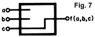
Therefore we can forget about a and b, and implement our black box as shown in
Fig. 7. We have grouped together the four adjacent squares to eliminate a and b.
Notice that we have simplified things a great deal, since we now need no gates
at all.
A key factor arises here. It isn't necessary to include all of these AND
functions, and the Karnaugh map tells us how to eliminate some of the terms. For
example, looking at Fig. 6, we see that f(a,b,c) is a one for four adjacent
boxes forming the bottom half of the map. (We will consider squares on opposite
edges to be adjacent.) It is also easy to see the following: The only variable
which does not change as we go from one square with a one to another with a one
is c. It remains at one. What this means is that f(a,b,c) cannot depend on a and
b because, regardless of their values, f(a,b,c) is a one as long as c=1.
Therefore we can forget about a and b, and implement our black box as shown in
Fig. 7. We have grouped together the four adjacent squares to eliminate a and b.
Notice that we have simplified things a great deal, since we now need no gates
at all. 
 Maps of one, two, three, and four variables are shown in Fig. 8. Maps of one
variable are rarely used, and maps with more than four variables are seldom
needed - even if such a problem were to chance along, the Karnaugh map would not
be the tool to use. Its value depends on the pattern recognition capability of
the user, and it becomes hard to recognize pattern groupings in maps of more
than four variables.
Maps of one, two, three, and four variables are shown in Fig. 8. Maps of one
variable are rarely used, and maps with more than four variables are seldom
needed - even if such a problem were to chance along, the Karnaugh map would not
be the tool to use. Its value depends on the pattern recognition capability of
the user, and it becomes hard to recognize pattern groupings in maps of more
than four variables. 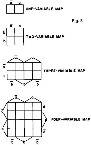
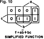 Rule 3: The same
procedure holds for eight, sixteen, and so on, adjacent boxes. Each box in a
grouping must be adjacent to three, four, etc., others within that group.
Rule 3: The same
procedure holds for eight, sixteen, and so on, adjacent boxes. Each box in a
grouping must be adjacent to three, four, etc., others within that group. 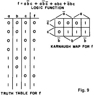 To illustrate, the Karnaugh map of Fig. 9 is repeated in Fig. 10, along with
the adjacency groupings and the resulting simplified function. Note the contrast
in simplicity. The boxes represented by abc and a
To illustrate, the Karnaugh map of Fig. 9 is repeated in Fig. 10, along with
the adjacency groupings and the resulting simplified function. Note the contrast
in simplicity. The boxes represented by abc and a
 Let's return to our newly developed map technique now and develop the
(clocked) J-K flip-flop as a last example. For convenience, since output changes
are allowed only on clock transitions, let's denote the unstable state q by Qn
and the stable state Q by Qn+1. This is reasonable, because Qn
is the stable state just prior to the nth 1-0 clock transition, and is the
unstable state just afterward, with the flip-flop settling down into the stable
state Qn+1 before the next clock transition occurs.
Let's return to our newly developed map technique now and develop the
(clocked) J-K flip-flop as a last example. For convenience, since output changes
are allowed only on clock transitions, let's denote the unstable state q by Qn
and the stable state Q by Qn+1. This is reasonable, because Qn
is the stable state just prior to the nth 1-0 clock transition, and is the
unstable state just afterward, with the flip-flop settling down into the stable
state Qn+1 before the next clock transition occurs.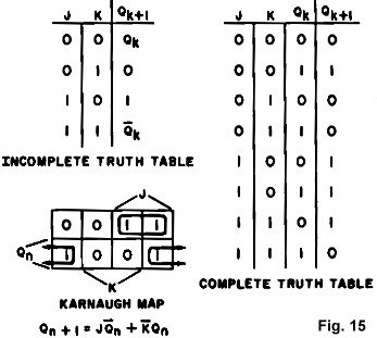

|
||||||||||||||||||||||||||||||||||||