|
|||||||||||||
 |
|||||||||||||
Microelectronics Circa 1963
|
|||||||||||||
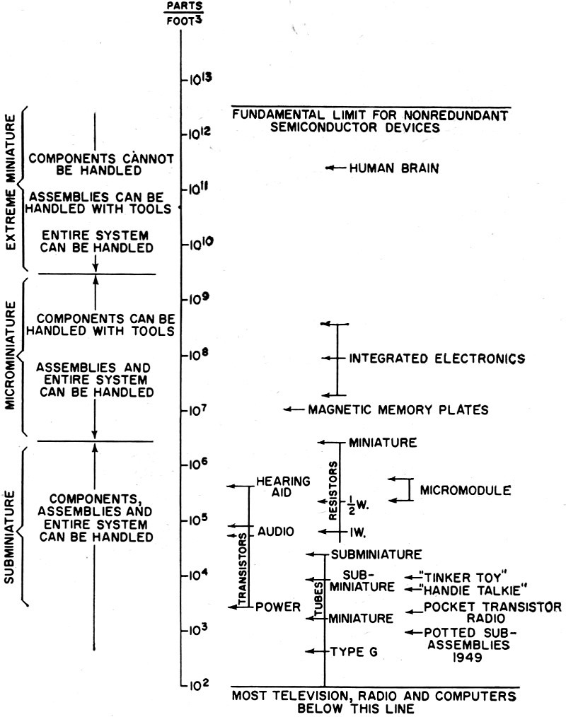
It seemed weird to read of microelectronics device density expressed in parts per cubic foot of semiconductor substrate. Describing density that way makes some sense when considering 3-dimensional devices with vertically stacked elements, but this was in a 1963 article in Electronics World magazine, so that could not have been the case. The motivation, evidently was to be able to compare microcircuit density with that of the human brain in terms of neuron density. In fact, there is an interesting chart presented that shows the evolution in circuit density beginning with vacuum tube circuits, progressing through the state of the art in 1963, projecting for future years, and finally peaking with the brain's density. Interestingly, the brain density shows as about 5x10¹¹/ft3, while the "nonredundant semiconductor device" limit is 1013/ft3. Contemporary measurements estimate a neuronal density of around 4x10⁴/mm3 (1x10¹³/ft3), which is about a factor of 10-20 over a span of 50 years (not too bad). I gave up trying to find useful data on current transistor density in volumetric units, but in terms of devices per mm2, Intel is running better than 30 transistors/mm2, which, although not really a legitimate exercise, translates to [√(30 transistors/mm2)]3 = 2x10² transistors/mm3. That means we're now at about 1/200th of the human brain density of 4x10⁴ neurons/mm3. Microelectronics Circa 1963
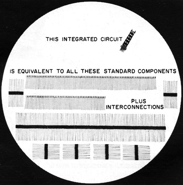
The electronics industry is on the verge of a new era with the introduction of integrated microelectronic circuits. This new concept, now in active development by a score of laboratories, can pack over a million parts into a cubic foot of space and, at the same time, greatly increase reliability. Already circuits are available in quantity, in packages only 0.3 inch in diameter and 0.2 inch high, to build complete logic and arithmetic sections of computers. The world's first integrated-circuit electronic control computer was announced last May. Called "Martac 420," the new computer was built by the Martin Company at Denver, Colorado. Designed primarily for ICBM pre-launch checkout and control, it tests and computes the readiness of all electronics in the missile. Within the electronic computing system, traditionally made up of transistors, diodes, and resistors, is logic circuitry comprising only plug-in integrated circuits. These reduced a conventional 20,000 parts to 5000 and cut over-all size to three-eighths that of previous construction. One part of this system, a decade counter with direct-coupled circuitry, is shown in Fig. 2. Here the integrated-circuit counter is compared to the number of conventional parts that might have been used.
New integrated circuits being worked on in a score of laboratories promise fantastic size reduction of much equipment, more reliability, and, eventually, low cost.
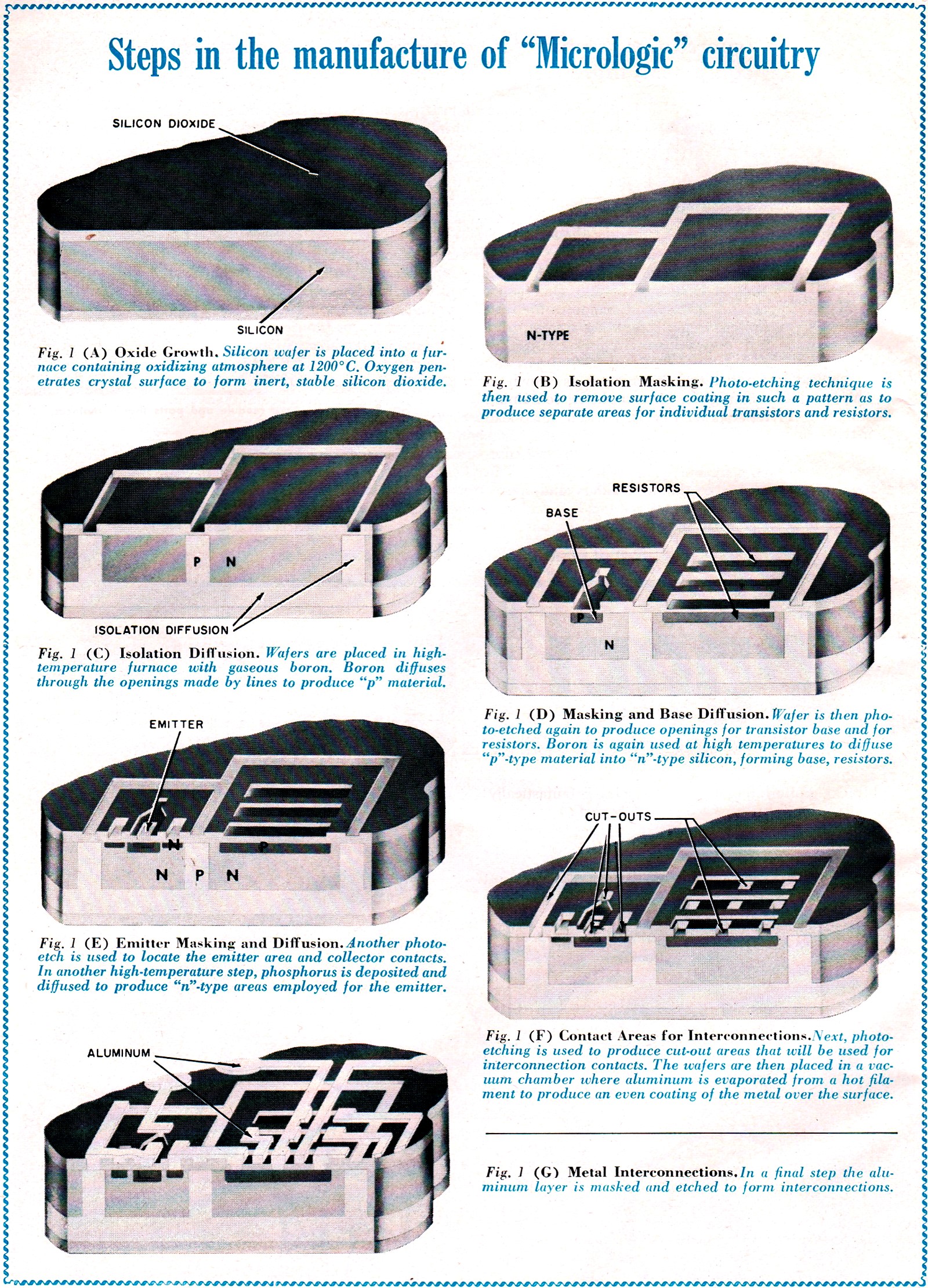
Steps in the manufacture of "Micrologic" circuitry. Microelectronic development has been encouraged by the needs of military and space programs. Millions of dollars are now being spent for research and development. But, as in other areas of military research, benefits will eventually be passed on to the public. Military and space programs require smallness, reliability, and lightness; industry wants low cost and reliability; the public wants low cost. Microelectronic integrated circuits offer all these things. Their appearance in all types of equipment, military and consumer, awaits only the ability to make the wide variety of circuits needed. To visualize the future scale of sizes compared to present and past equipment, the graph of Fig. 3 shows theoretical parts per cubic foot, ranging from World War II electronic equipment to the human brain. It is difficult to conceive the ultimate theoretical smallness, but the human brain is probably close to this limit, having a density of over 100 billion parts per cubic foot. Integrated circuits should perhaps more rightly be called functional blocks, because each is a single device performing a complete electronic operation. Such functions might include one or more stages of amplification, or several switching stages to perform a computer logic step, such as storing numbers or counting. Fig. 1 (A) Oxide Growth. Silicon wafer is placed into a furnace containing oxidizing atmosphere at 1200°C. Oxygen penetrates crystal surface to form inert, stable silicon dioxide. Fig. 1 (B) Isolation Masking. Photo-etching technique is then used to remove surface coating in such a pattern as to produce separate areas for individual transistors and resistors. Fig. 1 (C) Isolation Diffusion. Wafers are placed in high-temperature furnace with gaseous boron. Boron diffuses through the openings made by lines to produce "p" material. Fig. 1 (D) Masking and Base Diffusion. Wafer is then photo-etched again to produce openings for transistor base and for resistors. Boron is again used at high temperatures to diffuse "p"-type material into "n"-type silicon, forming base, resistors. Fig: 1 (E) Emitter Masking and Diffusion. Another photo-etch is used to locate the emitter area and collector contacts. In another high-temperature step, phosphorus is deposited and diffused to produce "n"-type areas employed for the emitter. Fig. 1 (F) Contact Areas for Interconnections. Next, photo-etching is used to produce cut-out areas that will be used for interconnection contacts. The wafers are then placed in a vacuum chamber where aluminum is evaporated from a hot filament to produce an even coating of the metal over the surface. Fig. 1 (G) Metal Interconnections. In a final step the aluminum layer is masked and etched to form interconnections. Various Design Techniques One form of microelectronic circuit in common use today is made from a single silicon semiconductor crystal, with no external circuit wiring or components. Wiring is thus reduced to between-circuit interconnections, which may be printed boards. A typical integrated functional block is shown in Fig. 4. This is a half-shift register for computers, containing 9 transistors and 14 resistors all mounted within an 8-lead transistor-type can. Intermediate approaches to microelectronics usually comprise the high-density packing of components, either on or in wafer substrates, or bunching components together like cordwood with welded connections. Another technique, called "thin film," involves the evaporation of desired metals on the substrate. With suitable masks or stencils, and the right choice of metals, it is possible to form all of the passive components (resistors, capacitors, and inductors) plus interconnecting wires. But it is still necessary to insert individual transistors and diodes.
Fig. 2 - Decade counter module and parts that it replaces.
Fig. 3 - Packing density for systems and components.
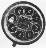
Fig. 4 - "Micrologic" element containing 9 transistors and 14 resistors on base 70 mils square, which is then inserted into the 8-pin transistor case illustrated at the right.
Fig. 5. "Micrologic" element shown mounted in transistor case (enlarged 6 times). The most promising microelectronic concept at present, for versatility in serving both computer and communication needs and practical to construct with present scientific knowledge, seems to be the solid-state integrated functional block. Maximum Reliability For military and space electronics the reliability consideration is probably uppermost. Electronic systems used with weapons, aircraft, communications, and the control, launching, and tracking of orbiting or space vehicles, is fantastically complicated and will be more so in the future. For example, the over-all reliability of a system equals the product of the reliability of each of its parts. If the system has three parts, each with a 90 percent chance of success, then the chance of the system for successful operation is (0.9 x 0.9 x 0.9 = 0.73) 73 per-cent. With perhaps billions of components involved in multi-million dollar space shots and with men's lives at stake, the expectation of success must be very much greater than that and the problem is infinitely more complex. Experience has shown that deep inspection and extensive quality control are still not adequate to assure high reliability. Costs are too high and errors can be introduced into the controls themselves. Therefore, a reduction in the number of individual components, by making them part of an integrated circuit, is the only practical way to meet this urgent need. Putting it another way, the more components, the greater the chance of failure. Fabricating the Circuit To make an integrated functional circuit, which will provide the active functions of diodes and transistors as well as the passive components, one begins with a material having semiconductor potential, such as silicon. The properties necessary for semiconductor electrical characteristics then require the introduction of impurities into the silicon crystal. These impurities become the current carriers, since the pure crystal is not a good conductor. The atoms of the impurity must be able to combine with the crystal structure in such a way that an electron is either added or taken away. The first impurity type is called n and the latter p, for negative and positive. (After Wallmark and Marcus, "Proceedings of IRE," March, 1962) If p and n characteristics are formed alternately in the same material, then an electrical barrier is formed. This barrier will allow current to flow readily when a battery is placed across it with the negative terminal to the n type and positive to the p type. But on reversing the battery a high resistance is presented to current flow. With present technology, one efficient way of making integrated circuits with silicon is to introduce a small amount of n impurity into the entire ingot. Then the n polarity is either counteracted as required by the addition of p impurity, or the n characteristic is strengthened by increasing its concentration. In the manufacture of integrated circuits these impurities are added to the circuit substrates by diffusion. The units are placed in a high-vacuum furnace and, at an elevated temperature, a gas containing the desired impurity is introduced so that the impurity comes in contact with the substrate and penetrates its surface. Other methods of adding impurities to semiconductors, such as alloying, are not suitable for integrated circuits. The diffusion method is the same as used for the manufacture of modern high-frequency silicon transistors. The great advantage of the diffusion method is that many units can be placed simultaneously in the furnace to make thousands of devices. With all being exposed to the same conditions, their uniformity is high, and production yields are high, because once the process is perfected each individual device tends to be as good as the whole. The patterns of diffusion on the substrates are formed by a photolithographic process similar to that used for etching plates in printing. Very fine details are possible, limited only to the degree of control over the precision camera work, the making of masks for the patterns, and the alignment of the masks in successive manufacturing steps. Both active and passive components are made into the silicon substrate material by the same diffusion processes. The methods employed for the several types of components follows: 1. Resistance is controlled by varying the amount of diffusion of impurities. More impurity lowers resistance. The photolithography pattern determines length and width. 2. Capacitors are formed in two ways. In one method, p-n junctions (barriers) are used, which inherently exhibit capacitance when reverse biased. In the second method, capacitors are formed on the surface, with silicon dioxide acting as the dielectric. 3. Inductors of limited value can be formed by diffusing-in a heavy concentration of an impurity in a spiral pattern. Considerable development is still required in this area, however. 4. Transistors and diodes are made by successive diffusion of their parts. These can be made at the same time as the passive parts, if the impurity concentrations are the same. "Micrologic" Manufacturing Typical microelectronic integrated circuits, known as "Micrologic" by Fairchild Semiconductor, are made by means very similar to those used for diffused "planar" transistors. This is a device whose surface is in one plane, with the base and emitter contacts on the upper surface, and the collector integral with the substrate material. The previous generation of transistors was the "mesa" type, which involved etching away of the surface to control and reduce the size of the base area. True planar transistors have a hard protecting surface of silicon dioxide, formed by an oxidizing atmosphere introduced with the diffusions. The "Micrologic" manufacturing steps, from the preparation of the ultra-pure silicon crystals to final inspection and capping, are shown in Figs. 1 and 5. Some 60 to 100 circuits are formed simultaneously in one wafer, and dozens of wafers can be diffused at one time. This batch processing leads to lower and lower costs. The completed unit with leads attached is evaluated for reliability and electrical performance, by a unique method of testing. Since individual components cannot be tested, the entire function is checked for performance over the specified voltage and temperature ranges . Of the several approaches to micro-electronics now under investigation, the integrated circuit seems to have an excellent chance of long-range and universal use. Reasoning behind this statement is the integrated circuit advantages of inherently high reliability, the ingredients required for mass production, and consequently, low cost. Other types will have varying degrees of popularity. The microsized discrete component may lose favor when integrated circuit development permits all desired functions to be served by them. The drawbacks of the discrete micro-component approach are failure to reduce the number of interconnections and high cost. Thin-film circuits will logically be used with integrated circuits to give greater flexibility and a wider range of circuit values than possible with diffusion alone. But with advanced integrated circuit technology, the thin-film circuit with individual transistors and diodes will no longer be required. Admittedly, however, the transistor was announced only 14 years ago and we have probably only scratched the surface of the potential capability, materials, and technologies. Already gallium arsenide is being investigated for its higher frequency potentiality. Cryotrons, which switch at zero resistance with very low temperatures, have been found adaptable to thin-film production. And the field-effect transistor is coming into its own as a high-impedance amplifier, competing with vacuum tubes. The success of the integrated circuit principle, however, whether in the form described here or in some form yet to be discovered, seems to be assured, because of the needs of our modern electronic world. It is not too farfetched to visualize them in all types of industrial and consumer equipment in the next five years or so. They will probably be seen in broadcast and communications equipment, in hi-fi gear, in household electronic controls, and in small business computers. |
|||||||||||||
 |
|||||||||||||
|
|||||||||||||
 By William O. Hamlin / Fairchild Semiconductor
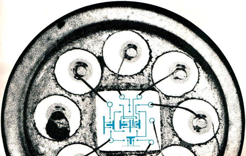


|
||||||||||||||||||||||||||||||||||||