|
|||||||||||||
 |
|||||||||||||
Gunn Oscillators
|
|||||||||||||
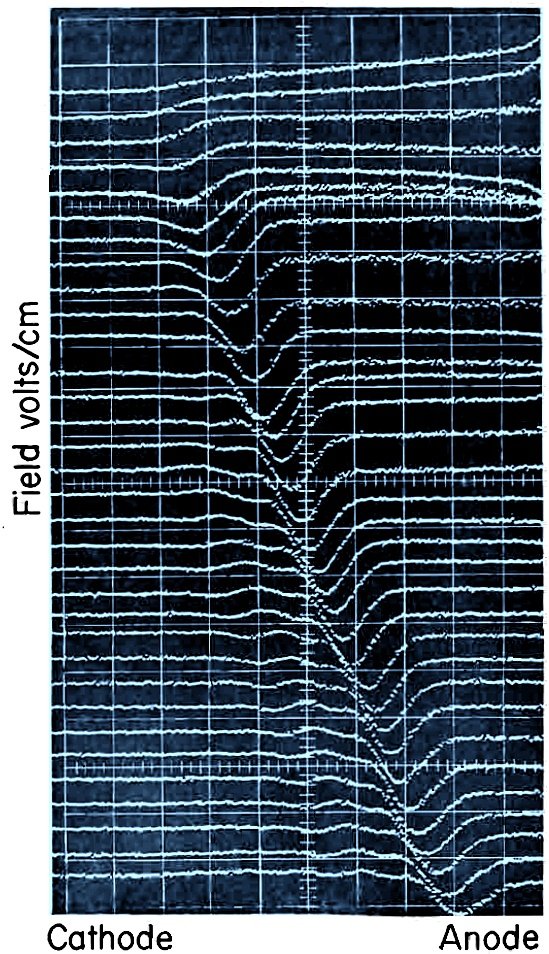
This 1967 Electronics World magazine article highlights a potential revolution in microwave technology through new semiconductor devices that could miniaturize and drastically reduce the cost of microwave sources. The focus is on two promising devices: the Read p-n junction diode and the Gunn bulk gallium arsenide oscillator. The Gunn device, discovered accidentally by Dr. J.B. Gunn at IBM, operates on a radical principle - a bulk semiconductor material oscillates at microwave frequencies without external tuned circuitry when a threshold voltage is applied. Key to the Gunn effect is the unique property of gallium arsenide, which features a second conduction band. Electrons entering this high-energy, low-mobility band create "domains" that drift slowly from cathode to anode, causing current oscillations. This generates microwave frequencies based on the domain's transit time across the material. Though simpler and cheaper than existing devices, the Gunn oscillator faced challenges in power output and reliability. The article concludes that while it was uncertain which device would dominate, the Gunn effect represented a significant breakthrough poised to enable new consumer microwave applications. Note the "waterfall" chart in Figure 3, which was not referred to as such because the term did not appear until the 1990s when finance and management firms coined the name. Gunn Oscillators
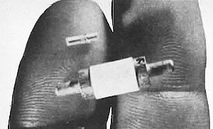
The larger device is intended for the Gunn bulk oscillator, while the smaller device houses a Read-type junction diode By David L .Heiserman A new type of microwave semiconductor that may one day replace present complex and expensive sources, and create new consumer microwave communications and radar devices. There is little doubt in the minds of semiconductor scientists and engineers that microwave technology is on the threshold of a miniaturization and cost revolution. A new breed of simple microwave semiconductors may one day replace our present complex and expensive microwave sources and create a whole new line of consumer microwave communications and radar devices. The makers of the revolution will be the new transit-time semiconductors best represented by the Read p-n junction diode and the Gunn bulk gallium arsenide oscillator. ( See "New Frontiers in Semiconductors" on page 78 of the March, 1967 issue.) At this stage of development, however, no one can say which device will eventually set the micro-wave revolution into motion - both have advantages and disadvantages, and both are plagued by production reliability problems. The theories of operation of both devices are rather new. The Read-type device operates on the well -known principles of the zener and tunnel diodes with the new idea of semiconductor electron transit time tying the two effects together. The operation of the Gunn device, however, represents a radical departure from conventional semiconductor thinking. In this respect, the Gunn device is worthy of closer study.
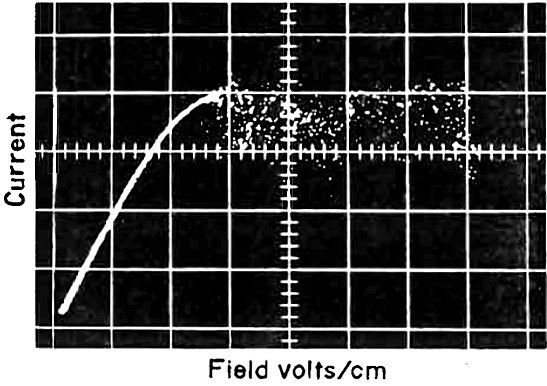
Fig. 1 - The current through bulk GaAs increases with an increasing amount of applied d.c. voltage until the conduction band electrons gain enough energy to skip upward into high energy, low-mobility band. At this threshold voltage (about 3000 volts /cm or about 6 volts of applied voltage) the GaAs sample will oscillate without any external tuned circuitry.
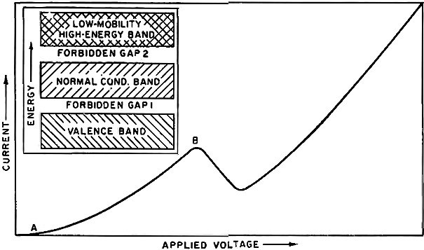
Fig. 2 - The quantum- energy diagram (shown in the inset) along with a corresponding current-voltage curve for bulk gallium arsenide are illustrated below. The existence of the second forbidden gap and the low- mobility, high- energy conduction band gives GaAs quite different properties from the usual semiconductor, such as n -doped silicon, showing no negative R.
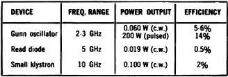
Table 1 - Performance of Gunn and other microwave devices. Gunn's Discovery Those of us who have been working in electronics for more than a few years associate semiconductor devices with one or more p-n junctions. We think in terms of holes and electrons, minority and majority carriers, junction potentials - always in terms of at least one pair of p and n semiconductor materials within one device. To think of an operational semiconductor made up of only one type of semiconducting material (a bulk semiconductor) is, traditionally, to think of an impossibility. Despite conventional thinking, the "impossible" was accidentally discovered by Dr. J.B. Gunn at IBM's Watson Research Center. In 1963, Gunn was running a series of routine experiments on a 0.005-inch thick slice of homogeneous n -type gallium arsenide when he noticed some unexpected coherent r.f. oscillations on his oscilloscope. Checking the setup for possible stray reactance or faulty components, he discovered that the plain n-doped material was oscillating at slightly less than 1 GHz (1000 MHz) with nothing more than a 6-volt d.c. power supply connected to the terminals (Fig. 1). What had been a purely theoretical possibility became a fact - Gunn found a semiconductor material that could oscillate in the microwave region without benefit of external tuned circuitry. Gunn and his associates soon realized that they had uncovered a phenomenon that could not be explained in terms of the usual semiconductor theories, so they were forced to try new theories and experimental techniques. The theoretical model of the oscillator, as finally developed, represents one of the biggest sidesteps from the mainstream of semiconductor thinking since the introduction of the laser diode. Negative Resistance in Bulk GaAs Without the benefit of the usual p-n junction, the Gunn oscillator demonstrates negative resistance properties. The quantum energy diagram and corresponding I-V curve are shown in Fig. 2. The diagram shows the usual forbidden gap between the valence and normal conduction bands. These regions in GaAs have the characteristics of any other n-type semiconductor such arsenic-doped silicon. The GaAs, however, has an additional forbidden gap and a special conduction band that differs from the first in two important respects. First, carriers (electrons in the case of GaAs) can cross the second forbidden gap only when the applied d.c. potential reaches an extraordinarily high value of 3000 volts per centimeter. Second, carriers that do gain enough energy to skip into the second conduction band effectively gain some mass and thus travel much more slowly through the semiconductor than their lower energy counterparts in the first conduction band. The second conduction band is thus described as one containing only high-energy carriers which travel with un- usual slowness through the semiconductor. It is this additional conduction band that makes it possible for an n -type bulk semiconductor to show negative resistance. Referring to the I-V curve in Fig. 2, the nonlinear slope between points A and B is due to the increasing fraction of valence electrons skipping upward into the high-mobility first (normal) conduction band under the influence of a small applied voltage. As the applied e.m.f. is increased beyond point B, however, the current drops off sharply. It is at this point that some of the electrons in the low-energy, high -mobility first conduction band enter the high-energy, low-mobility second conduction band. If electrons move slower in the second conduction band than they can in the first, it follows that increasing the percentage of electrons in the second conduction band will cause a corresponding decrease in the net rate of electron flow through the material. As the applied voltage passes beyond point B, then, the current through the GaAs sample decreases. This, of course, is the general description of a negative- resistance effect.
Fig. 3 - The low-mobility, high-energy electron domain passing through the Gunn device. The domain builds up near the cathode and moves with relative slowness to the anode, holding the current through the semiconductor to a minimum. Although the ordinate of the oscillogram is in terms of field strength, the downward progression of traces has no physical meaning except to display the chronology of the shock wave that is produced. The negative-resistance, junction-type semiconductors in use today require some capacitance or inductance to sustain oscillation while the Gunn device does not. So, negative resistance in bulk semiconductor theories are potentially useful, but cannot wholly account for the Gunn effect. Electron Domain Transit Time Electron Domain Transit Time The theory that finally rounded out the explanation of the Gunn effect involves the new concept of slow-moving, high-energy packets or "domains" within a bulk semiconductor. If a sufficient voltage (the threshold voltage) is applied to a thin slice of n-type GaAs, electrons skipping into the second conduction band tend to collect into discrete energy domains. Further, if the GaAs is of sufficient purity and the applied voltage is carefully regulated, one and only one domain can exist within the material at any one instant. Since this one domain is made up of second conduction band electrons, the domain will behave exactly as the electrons described in connection with Fig. 2. The domain will drift with relative slowness from cathode to anode, holding the net current flow through the semiconductor to a minimum. Once the domain reaches the anode, it disappears momentarily and current surges through the material via the first conduction band. This surge continues until another high-energy, low-mobility domain forms at the cathode. The current through the bulk semiconductor, then, is low during the electron domain transit time and relatively high during the brief period of time it takes to form another domain at the cathode. Thus, the Gunn device demonstrates current oscillations, the period of which depends on the rate of domain travel and the physical length of the bulk semiconductor material. The oscillogram of Fig. 3 shows the high-energy domain passing through discrete points along the length of a thin slice of bulk GaAs. The trace at the top shows the domain leaving the cathode. In the following traces, the moving electron domain is shown at points progressively closer to the anode. If the frequency of oscillation is assumed to be about 1 GHz, the traces cover an interval of about 1 μs. At the present stage of semiconductor technology, the Gunn device's advantages of small size, low cost, and simplicity must be weighed against the disadvantages of lower operating frequency and low c.w. output power. Placed beside the Read-type devices, the Gunn oscillator has about a 50 percent chance of becoming the microwave source of the future. See Table 1. Regardless of the final outcome, the Gunn effect described in this article represents another opening to products and industrial equipment thought impossible a few years ago. |
|||||||||||||
 |
|||||||||||||
|
|||||||||||||


|
||||||||||||||||||||||||||||||||||||