|
|||||||||||||
 |
|||||||||||||
Avalanche Transistor Circuits
|
|||||||||||||
Avalanche breakdown in semiconductors, initially viewed by engineers as a destructive limitation, was later discovered to be nondestructive when peak power was controlled through external circuitry. This 1967 Electronics World magazine article explains how avalanche transistors evolved from being considered problematic to becoming valuable components for high-speed pulse generation. Early adoption was hindered by inconsistent performance between transistors, requiring careful selection for reliability. Improved fabrication techniques reduced surface leakage currents, enabling modern avalanche transistors to operate at high collector voltages with sub-nanosecond rise times. These devices could produce impressive outputs - 75 volts and 10 amps in under 0.5 nanoseconds - with repetition rates reaching MHz ranges. The article details the avalanche multiplication process where electrons accelerated by high electric fields create carrier multiplication through impact ionization. Practical applications included sampling oscilloscopes, nuclear instrumentation, and laser modulation. Circuit configurations like emitter-follower setups and delay-line stabilization provided precise pulse control. The technology promised advancement into picosecond timing realms. A javascript "M" calculator is included. Note that the "M" curve in Fig. 2 does not follow the given equation. Diodes, Inc., still makes avalanche transistors such as the FMMT411Q, a silicon planar bipolar transistor designed for operating in avalanche mode for laser diode drivers, LIDAR, and high-speed pulse generators. Avalanche Transistor Circuits
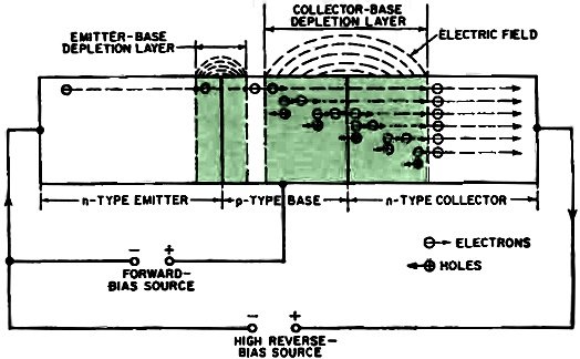
Fig. 1 - Simplified current-flow diagram of an "n-p-n" transistor that is shown here operating in the avalanche mode. By Sidney L. Silver These special switching transistors - made possible by improved fabricating techniques - can produce extremely fast pulses at high power output levels. In the early days of transistor development, avalanche breakdown was considered a troublesome phenomenon which imposed a limit on the useful life of a junction transistor. To offset this problem, collector voltages were restricted to values far below the actual breakdown rating in order to reduce surface leakage currents across the collector junction. Excessive leakage currents not only increased the power-dissipation level of the transistor, but also initiated thermal runaway and possible destruction of the device. The avalanche effect was found to be nondestructive it the peak and average power dissipated at the collector junction were controlled by external circuitry. By operating ordinary high-frequency switching transistors in the avalanche mode, it was possible to generate extremely fast pulses (in the nanosecond range) in applications requiring high current outputs of short duration. Nevertheless, the avalanche process did not find wide acceptance since, in many cases, transistors of the same type did not always exhibit uniform avalanching properties. Consequently, it was necessary to carefully test and select these units for consistent break-down characteristics, thus making it difficult to design stable, reliable pulse circuits. As a result of recent improvements in fabrication technology (leading to, for example, the reduction of surface leakage currents), modern avalanche transistors are now capable of operating at relatively high collector voltages and of producing large current-voltage swings with sub-nanosecond rise times. Within the limits set by allowable power dissipation, pulse widths of 100 is are easily attained with repetition rates in the MHz region. In simple circuits, peak swings of 75 volts and 10 amps in less than 0.5 ns are obtainable with ultra-high-speed transistors whose geometry is optimized for avalanche switching. In more complex circuits, rise times of less than one us can be generated at peak powers in excess of 500 watts across very low impedance loads.
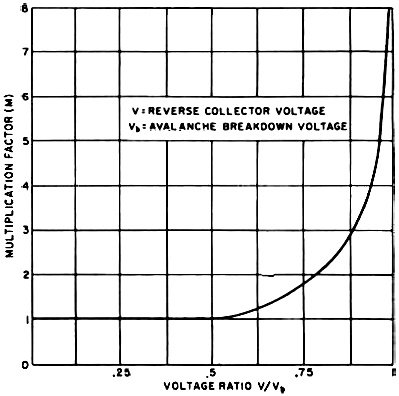
Fig. 2 - Relation between avalanche breakdown voltage and M. {Note: This curve does not jive with the M=1/[1-(V/Vb)n] formula!} Some of the important applications of avalanche transistors include the generation of fast- rising pulses employed in sampling oscilloscopes, decade ring counters, and high-speed nuclear instruments. For pulse power requirements in the milliwatt range, suitable avalanche devices are now being developed for low-level computer logic circuits. For higher pulse handling capacity, avalanchers are finding increasing use in strobe-pulse generators, pulse amplitude detectors, memory-core drivers, and voltage-comparators. With proper impedance-matching, avalanche pulse generators can be used for pulse modulation of injection lasers. In normal transistor operation, a reverse bias is applied to the base-collector junction so that an electric field is produced within a space charge region, or depletion layer, of the junction. In the avalanche process, however, the reverse collector voltage is raised substantially above the normal operating value so that the depletion layer is considerably widened, and a large electric field extends over most of the base region. As shown in Fig. 1, the strong electric field approaches the small field associated with the narrow emitter-base depletion layer thereby reducing the effective base width. As a result electrons diffuse across the base from the emitter region and accelerate to high velocities toward the collector. Upon entering the collector-base depletion layer, the fast-moving electrons excite additional carriers (hole-electron pairs) by impact ionization with atoms in the semiconductor material. Owing to the high field, the free electrons move rapidly toward the collector and the associated holes drift in the opposite direction across the base region. The new carriers, in turn, acquire sufficient energy to cause further ionization by collision with the other atoms in the material. Since the atoms in the lattice structure are closely spaced, the ionization process occurs many times, particularly at the collector-base junction which corresponds to maximum-field intensity. Avalanche Multiplication Factor (M) CalculatorThe cumulative process, referred to as avalanche multiplication, results in a much larger number of electrons entering the collector region than cross the collector-base junction. When a critical point is reached, the current flowing across the collector-base junction rises abruptly as avalanche breakdown occurs and tremendously high values of reverse collector currents are attained. The breakdown condition is not a permanent effect since the junction will rapidly recover when the voltage is reduced again. An important parameter used to designate the rise of collector current prior to breakdown is the multiplication factor (M), which is defined as the ratio of actual collector current to the current that would flow had there been no increase in current due to ionization. Fig. 2 shows a typical multiplication factor curve for an n-p-n silicon transistor in which M values are plotted against collector voltage. At low collector voltages, M is close to unity and no apparent multiplication effect is present. In avalanche, however, the emitter-to-collector gain is increased to a magnitude many times greater than unity, so that M approaches an infinitely high value. In practice, the multiplication factor can never be infinite, since this would imply an unlimited current flow and unlimited heat generation. To obtain a high value of M, it is desirable that the collector current be as large as possible; but a limit is set by the maximum allowable power dissipation of the transistor, which is controlled by external circuitry. The multiplication factor is found to be related to the reverse bias across the
collector junction by the formula:
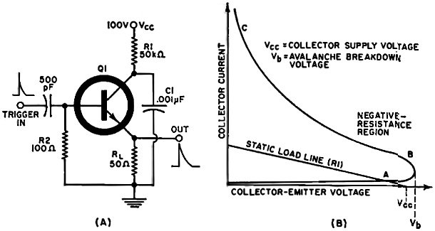
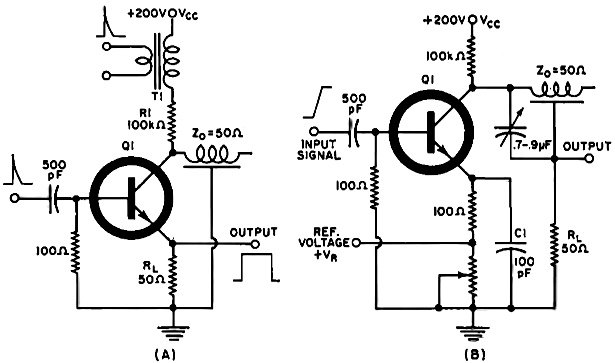
Fig. 3 - (A) Avalanche switching circuit, and (B) the V -I curve. Basic Circuitry The basic features of a single n-p-n transistor operating in the avalanche mode are shown in the emitter-follower configuration of Fig. 3A. In the quiescent state, capacitor C1 charges toward the collector supply voltage, Vee, which is adjusted to a value slightly less than that required to initiate avalanche breakdown. When a positive-going trigger pulse is applied to the base, the emitter-base junction becomes forward-biased, and the breakdown potential is effectively lowered. The emitter begins to inject electrons into the base, which are multiplied at the collector junctions, causing a regenerative current build-up to occur. At breakdown, the heavy current flowing through the collector-emitter junction path rapidly discharges C1 and produces the leading edge of a positive pulse across load resistor RL. The breakdown condition exists as long as there is stored energy in C1 to sustain it, since the alternate path ( from Vee via R1) is unable to supply sufficient current. After C1 has discharged, a small transient current flows through R1, which maintains the collector at a lower voltage and allows the transistor an interval of time to recover and revert back to its original quiescent state. Finally, capacitor C1 slowly recharges toward the collector supply source through R1 and upon arrival of the next trigger pulse, and the cycle is repeated. The pulse repetition rate of the monostable circuit in Fig. 3A is determined by the time constant of R1 and C1, while the pulse width depends upon the values of RL and C1. Resistor R1 can be made adjustable (within small limits) so that increased repetition rates are obtainable by decreasing its value. C1, which determines the avalanche turn-on transient, is usually fixed by pulse -width requirements. If a negative output pulse is required, the emitter terminal may be grounded and the load resistor, RL, is placed in series with the C1-to-ground connection. To convert the generator into a self-running type, the collector supply voltage, Vee may be raised or the base resistor, R2, returned to a suitable bias voltage so that the avalanche breakdown is achieved without the need for an external trigger. The sequence of events relating to the avalanche-switching mechanism is graphically illustrated by the volt-amp characteristic curve of Fig. 3B. Under quiescent conditions, a static load line is constructed to yield a single stable operating point (A), where it intersects the curve in the low-current region. When a trigger pulse appears, avalanching occurs between points A and B, where the transistor's operating point is shifted beyond its normal-region rating. Capacitor C1 supplies the surge of discharge current which builds up rapidly toward point C in the negative-resistance region. It is the low transit time with which the transistor switches from a low-current state to an avalanche discharge state in the negative- resistance area that leads to extremely fast rise times. When the trigger pulse has dissipated, the operating point moves back to point A as capacitor C1 recharges to the same point and the circuit is ready to accept another transient. An important design consideration is that the load line must not intersect the transistor breakdown curve in the high-current region. This condition, referred to as "latch-up," would establish an undesirable stable operating point at the common intersection and prevent the normal shift to point A during the recovery period. If the product of current and voltage at the latching point were sufficiently high to exceed the maximum transistor power rating, circuit malfunction or thermal destruction would occur.
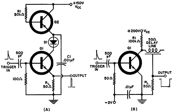
Fig. 4 - (A) A narrow-pulse avalanche generator capable of high pulse repetition rates. (B) Delay-line avalanche-mode generator.
Fig. 5 - (A) Pulse-coincidence detector. (B) Comparator circuit. Narrow-Pulse Switching The main disadvantage of the single-stage avalanche pulse generator is the relatively long recovery time after the avalanche transition period which sets a limit on the maximum pulse repetition rate. Fig. 4A shows an arrangement which incorporates a second transistor to dynamically reduce the charging time constant of the circuit without appreciably affecting the static load line during the pulse period. Initially, the base-emitter junction of transistor Q2 is forward biased, and C1 is charged, via Q2, toward the collector supply voltage, Vee. Transistor Q1 rests near its avalanche breakdown potential and Vee. is adjusted to a value slightly less than that which would start the Q1 circuit free-running. When Q1 is triggered C1 discharges rapidly through the series path formed by load resistor RL, transistor Q1, and diode Dl. The resultant voltage drop across Dl reverse-biases the emitter-base junction of Q2, leaving only the limiting resistor R1 as the current path between Vee, and the collector of Q1. After C1 has discharged, Q2 turns "on" and C1 rapidly charges toward Vee via the low-resistance path provided by Q2. By this means, very narrow pulses are easily generated which have fast fall times as well as fast rise times. Pulse repetition rates can thus be increased a hundredfold over the single-stage circuit, with obtainable repetition rates up to approximately 5 MHz. Delay-Line Stabilization In applications requiring flat-topped pulses, a transmission-line load provides greater control of pulse duration, amplitude, and phase of the output signal than does the use of a load capacitor. Fig. 4B shows a monostable pulse generator which employs an open-circuited delay line as a pulse-forming network in the collector circuit of transistor Q1. In this configuration, a hold-off bias is applied to the base to maintain Q1 in the nonconducting state. During the "off" cycle the delay line acts essentially as a capacitive load which is charged to the collector supply voltage, Vee in conjunction with resistor R1. The application of a trigger pulse forward biases the base-emitter junction and produces a positive regenerative avalanche transient across the transmission line and load resistor R1. At this point, the switching transient travels along the delay line ( approximately 2 ns/ft), which now behaves as a resistive element equal to its characteristic impedance (Z = 50 ohms). When the pulse reaches the open end of the line it is reflected back to the source (in phase) since there is no resistive termination at the load end to absorb the energy. Upon returning to the collector, the pulse increases the voltage across the source end of the line and causes a reduction of the voltage across R,. By this means the collector current is reduced to a sufficiently low value to turn off the transistor regeneratively, thus terminating the pulse. In this circuit, the duration of the rectangular output pulse is equal to the two-way transit time of the delay line. Although small changes of pulse repetition rate can be produced by adjusting the values of Vee and R1, the repetition rate is primarily determined by the value of the transmission-line capacitance. To prevent ringing and undesirable reflections, R1, must be equal to or slightly less than the characteristic impedance of the line. Fig. 5A indicates how the avalanche process is applied to coincidence detection in high-speed nuclear instrumentation. In this arrangement, the two trigger pulses applied to the delay-line coincidence circuit are derived from a pair of nuclear scintillating counters. To detect the coincidence of both pulses, one half of the required pulse height is coupled to the collector of Q1 and the other half is fed to the base input circuit. The collector circuit parameters are selected so that the presence of both pulses is necessary in order to drive the transistor into avalanche and deliver an output. In the voltage comparator circuit shown in Fig. 5B, the input level of a ramp signal is compared with an adjustable positive voltage reference source VR in the emitter circuit. When the applied voltage ramp exceeds the threshold trigger level, avalanche breakdown takes place and the collector-emitter path of Q1 conducts heavily. The delay line then discharges around the loop formed by load resistor R1xx emitter bypass capacitor C1, and Q1 so that a large nanosecond pulse is produced at the output.
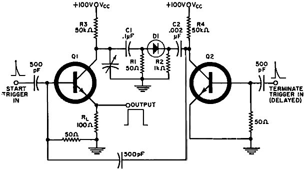
Fig. 6 - Variable-width avalanche pulse generator circuit. Variable-Width Pulse A convenient method of obtaining continuously variable pulse width is the complementary arrangement shown in Fig. 6. Here the fast rise time of avalanche transistor Q1 is utilized for the leading edge of the output pulse and that of Q2 for the trailing edge so that precise control of pulse duration is achieved. By varying the time delay between start and stop trigger signals, it is possible to continuously adjust the pulse width from a few nanoseconds to over one microsecond. Initially, C1 and C2 are charged toward the Vee source via resistors R3 and R4, respectively. To initiate the avalanche process, a start trigger pulse is applied to the base of Ql. A heavy current flows through the collector circuit which discharges Cl through the R1, RL, and Q1 path so that the leading edge of the output pulse is formed. During this interval, diode Dl is reverse-biased to prevent interaction with the Q2 switching circuit. After a predetermined period of time, a trigger pulse is applied to the base of Q2 in order to terminate the pulse. As C2 discharges through R2 and Q2 a large negative voltage is developed across R2 which overcomes the reverse bias on Dl. As a result, the R1-C1 junction is driven more negative so that the algebraic stun of the voltages between the Q1 collector and ground approaches zero. This bucking effect cancels the power that keeps Q1 in avalanche, thereby turning off Q1 and terminating the pulse. At this point C1 and C2 recharge to complete the cycle as the Q1 circuit awaits the arrival of a new start pulse. At the present state of the art, the avalanche mechanism adds a new dimension to solid-state switching design which has not yet been fully explored. To meet the increasing demands for ultra-high-speed, high-current switching applications, a number of high-frequency transistors are now commercially available, e.g., 2N3033, 2N3034, 2N3035, which are specifically tailored for avalanche-mode operation. As more avalanching transistors become available, circuit designs will reach farther into the picosecond region to solve some of the problems related to operation at very high repetition rates. |
|||||||||||||
 |
|||||||||||||
|
|||||||||||||


|
||||||||||||||||||||||||||||||||||||


