|
  As frequencies increase,
conduction begins to move from an equal distribution through the conductor cross
section toward existence almost exclusively near the surface. Depending on the conductor
bulk resistivity (δs), at sufficiently high frequency all the RF current
is flowing within a very small thickness at the surface. Furthermore, the current
concentrates nearest to the surface that abuts the highest relative dielectric constant.
Lower bulk resistivities result in shallower skin depths. As frequencies increase,
conduction begins to move from an equal distribution through the conductor cross
section toward existence almost exclusively near the surface. Depending on the conductor
bulk resistivity (δs), at sufficiently high frequency all the RF current
is flowing within a very small thickness at the surface. Furthermore, the current
concentrates nearest to the surface that abuts the highest relative dielectric constant.
Lower bulk resistivities result in shallower skin depths.
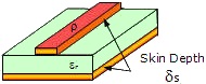 In the case of a microstrip
layout (to the left), the current concentrates nearest to the substrate dielectric
material, although current does also concentrate at the other surfaces as well (redder
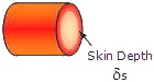
regions). For a solid wire (to the left), the current concentrates on the outer
surface. For this reason, when skin depth is shallow, the solid conductor can be
replaced with a hollow tube with no perceivable loss of performance. Choice of a
plating material can degrade performance (increase attenuation) if its bulk resistivity
is greater than that of the copper. In the case of a microstrip
layout (to the left), the current concentrates nearest to the substrate dielectric
material, although current does also concentrate at the other surfaces as well (redder
regions). For a solid wire (to the left), the current concentrates on the outer
surface. For this reason, when skin depth is shallow, the solid conductor can be
replaced with a hollow tube with no perceivable loss of performance. Choice of a
plating material can degrade performance (increase attenuation) if its bulk resistivity
is greater than that of the copper.
Most common conductors have a relative permeability of very near 1, so for copper,
aluminum, etc., a µ value of 4π* 10-7
H/m can safely be assumed. Magnetic materials like iron, cobalt, nickel, mumetals,
and permalloy can have relative permeabilities of hundreds or thousands.
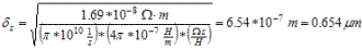
The equation for calculating the skin depth is given here:
(click
here table of
calculated values)

µ = permeability (4π* 10-7
H/m), note: H = henries = Ω*s
π = pi
δs = skin depth (m)
ρ = resistivity (Ω*m)
ω = radian frequency = 2π*f (Hz)
σ = conductivity (mho/m), note: mho [ ] = Siemen [S] ] = Siemen [S]
Example: Copper @ 10 GHz (ρCu=1.69*10-8 Ωm)
|