January 1962 Popular Electronics
 Table of Contents Table of Contents
Wax nostalgic about and learn from the history of early electronics. See articles
from
Popular Electronics,
published October 1954 - April 1985. All copyrights are hereby acknowledged.
|
Bypass capacitors play a
vitally important role in electronic circuit design. Many people do not know the
proper way for deciding which capacitor or capacitors is/are needed for effective
noise and/or signal bypassing without either overdoing or underdoing it. Needs change
over the years as frequencies and signal characteristics occupy new realms of the
spectrum. A Fourier analysis of some of today's complicated waveshapes for switching
power supplies shows how sometimes tailored responses to bypassing is required.
This article from the January 1962 Popular Electronics magazine does not
delve into the intricacies of complex filters, but it does provide a nice introduction
to the need for bypassing and how to stand a good chance of being successful at
it. In rare instances, no amount of bypassing will solve problems with spurious
signals and a more engineered approach is required where the functional circuit
needs to be modified (I know this from experience!).
Here is an article written by RF Cafe contributor
Carl Lodstrom on the subject of bypassing.
Getting to Know the... Bypass Capacitor
 By John M. Doyle By John M. Doyle
Technical Editor, National Radio Institute
Capacitors are used in modern electronic circuitry for such purposes as blocking,
filtering, timing, and bypassing. The last-mentioned application - bypassing - is
by far the most common. It's also much more critical than many people suspect, since
the selection of a wrong-value bypass capacitor can result in poor frequency response,
phase distortion, circuit instability, or even outright oscillation.
Now, you may feel that this problem is no concern of yours, but is rather one
for the design engineer. "Shucks," you say. "If a capacitor-bypass or otherwise
- goes bad, I'll replace it."
This approach works fine in most cases. But how many times have you wished you
could help fix a piece of equipment after a well-intentioned, but poorly instructed,
do-it-yourself fan has been hard at work with his trusty soldering gun? Or how many
times have you felt like throwing that cheap "screech-box" receiver out of the window,
when a 15¢ bypass capacitor would do much to quiet the demon of temptation? Finally,
remember that despite our ultra-modern manufacturing methods, "goofs" are still
made by people who do the physical wiring and inspection but who know nothing about
the workings of the circuit.
If you're now convinced of the importance of knowing a little more about bypassing
(and shame on you if you aren't), let's get on with the job.
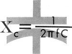
Reactance. When a capacitor is used as a bypass, it must provide
a low-impedance path for electrical currents of certain frequencies and a high-impedance
path for those of other frequencies. The property which permits it to operate in
this manner is called reactance. The value of reactance for a given frequency is
determined by the basic formula:
Xc = 1 / (2π f C)
where Xc is the capacitive reactance in ohms,
2π is a
constant (approximately 6.28), f is the operating frequency in cycles per second,
and C is the capacitance in farads.
This relationship tells us that the reactance of a given capacitor decreases
as frequency increases. For example, the value of Xc for a 0.01-μf.
capacitor at a frequency of 500 cycles is about 31,800 ohms. But at a frequency
of 5000 cycles, the reactance has decreased to about 3180 ohms.
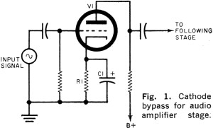
Fig. 1. Cathode bypass for audio amplifier stage.
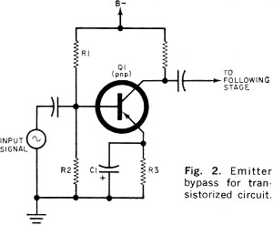
Fig. 2. Emitter bypass for transistorized circuit.
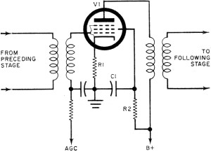
Fig. 3. Screen bypass for typical i.f. amplifier in a television
set.
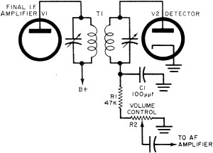
Fig. 4. R.f. bypass for diode detector stage.
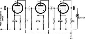
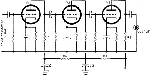
Fig. 5. Decoupling is required because of feedback through
R1 and R2.
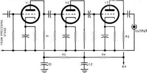
Fig. 6. Networks R4/C2 and R3/C1 prevent undesired feedback
between stages.

Fig. 7. Decoupling capacitors should be grounded at one
point for best results at high frequencies.
Not only must we be able to calculate Xc, but we must also know how
to determine what value capacitor is needed to obtain a certain reactance at some
specified frequency. All that we have to do is rearrange the above equation as:
C = 1 / (2π f Xc)
where all symbols have the same meaning as before. For example, if we want to
know what value capacitor will provide a reactance of 18 ohms or less at a frequency
of 500 cycles, we just substitute known values in the above formula. The calculated
answer is 17.7 μf., approximately, but the next highest standard capacitance value
available will be okay for most applications.
Audio-Frequency Amplifiers. In a typical audio-frequency amplifier,
such as that shown in Fig. 1, a capacitor, C1, is used to bypass audio frequencies
around the cathode resistor, R1. If capacitor C1 is omitted or if it does not operate
properly, the a.c. plate current component develops a voltage drop across R1 which
opposes the input signal applied to the grid. This effectively reduces stage gain
and results in inverse feedback or "degeneration."
Now, let's see what requirements are placed on the capacitor if it is to prevent
degeneration. Suppose the amplifier is to pass all frequencies between 100 and 5000
cycles, and the value of cathode resistor recommended by the manufacturer for class
A operation is 1500 ohms. Because the reactance of the capacitor decreases as frequency
increases, a capacitor that satisfactorily bypasses the resistor at the lowest frequency
will work quite nicely over the entire range.
A rule-of-thumb used by circuit designers is that the reactance of the capacitor
at the lowest frequency to be passed should not exceed one-tenth the value of the
resistor it bypasses. Using this rule, we substitute known values in the equation
developed for finding C:
C = 1/(6.28 x 100 x 150) = 11 μf
An electrolytic capacitor is suitable for this purpose because its leakage resistance
is not important and high capacitance is obtained in a compact size.
In some applications, such as high-quality audio amplifiers, the ratio of resistance
to reactance at the lowest frequency passed is made 20 to 1 or even higher, but
the ratio used in our example is adequate for most cases. Needless to say, the working
voltage of the capacitor selected for any bypassing applications must be larger
than the maximum voltage present.
Bypassing in the case of a transistorized audio-frequency amplifier is very similar.
A typical pnp transistor amplifier, using the common-emitter arrangement, is shown
in Fig. 2. Base bias is obtained from the voltage-divider network, consisting
of R1 and R2, and the emitter is forward-biased (negative in the case of a pnp transistor,
and positive for the npn type). To prevent signal degeneration, the emitter-bias
resistor (R3) is bypassed with a high-value electrolytic capacitor (C1).
In either type amplifier discussed above, a certain amount of degeneration is
sometimes intentionally used. Therefore, before jumping to any wrong conclusion,
always make sure that degeneration is in fact undesirable before attempting to correct
a case of "faulty" design. If bypassing is improved where degeneration is needed,
the circuit will not operate properly.
Other Applications. When a pentode-type tube is used, additional
bypassing is needed in the screen grid which must operate at ground potential, as
far as all signal voltages are concerned, if degeneration is to be avoided. A typical
case is the television i.f. amplifier shown in Fig.3.
In this circuit, screen potential is obtained from the plate-supply source through
the screen-dropping resistor, R2. If bypass capacitor C1 fails to operate properly
at any frequency, the gain of the amplifier falls off at that frequency. The value
of C1 is again determined by the rule-of-thumb that its capacitive reactance at
the lowest frequency passed should not exceed one tenth the value of the resistor
it bypasses.
Generally, mica or ceramic capacitors, ranging in value from about 50 μμf. to
0.01 μf., are used for r.f. bypassing arrangements of this type. If the pentode
is employed as an audio-frequency amplifier, high-quality paper or electrolytic
capacitors are used. Their proper value can be determined in the same way.
Sometimes it is necessary to bypass radio but not audio frequencies. A typical
case is in the detector circuit of an AM receiver, as shown in Fig. 4. Assuming
that the r.f. carrier frequency is 455 kc., if the reactance of C1 is to be one-tenth
the value of R1 at this frequency, its value - using the formula previously given
- is approximately 75 μμf. We would use a standard 100-μμf. mica or ceramic capacitor.
If the highest audio frequency to be passed is 5000 cycles, the reactance of the
capacitor at this frequency is better than 300,000 ohms.
Another circuit in which bypassing is important is illustrated in Fig. 5,
where three amplifier stages are fed from a common plate-voltage supply. Since most
power supplies possess a finite impedance, the output of V3 will be returned to
the plate circuit of V1 through load resistors R2 and R1. This effective signal
voltage is then fed to the grid circuit of V2 and then into V3. Naturally, if the
gain of these stages is high enough, oscillation occurs.
To prevent instability of this type, decoupling networks are used, a typical
example of which is shown in Fig. 6. The reactance of C1 and C2 at the lowest
operating frequency is made very small compared to the resistance of R3 and R4.
Because R3/C1 and R4/C2 form voltage dividers, almost the entire voltage developed
across the common impedance is dropped by R3 and R4. Essentially, no feedback voltage
is then coupled into the plate circuit of V1 or V2.
The values of R3 and R4 should be kept as low as possible to accomplish the job
without dropping a prohibitive amount of the d.c. plate voltage for V1 and V2. In
cases where a very small drop in this voltage is all that can be tolerated, R3 and
R4 can be replaced by an inductance of low d.c. resistance. The value of inductance
needed for a given reactance at a specified frequency is determined by the formula:
L = XL / 2π f
where XL is the inductive reactance in ohms, and f is the operating frequency
in cycles per second.
Chassis Grounds. Here's a final word about connecting bypass
capacitors. At frequencies of 30 mc. and below, the dimensions of the chassis are
usually only a fraction of a wavelength, and it can be considered a fixed reference.
Above 30 mc., however, the chassis is essentially a conducting sheet on which points
of maximum current and voltage appear.
In the circuit of Fig. 7, grid and plate "ground" currents pass through
the chassis to the cathode of the stage. A good practice, generally, is to separate
these ground currents from the chassis by returning all leads to the cathode or
a bus bar. Just be sure, however, that the leads are kept as short as possible to
prevent cross-coupling and undesirable feedback.
|