GSM Handset Power Amplifier Control Loop Design |
|||||||||||||||||||||||||||||||||||||||||||||||||||||||||||||||||||||||||||||||||||||||||||||||||||||||||||||||||||||||||||||||||||||||||||||||||||||||||||||||||||||||||||||||||||||||||||||||||||||||||||||||||||||||||||||||||||||||||||||||||||||||||||||||||||||||||||||||||||||||||||||||||||||||||||
|
GSM Handset Power Amplifier Control Loop Design An Analog Approach by Jason Millard & Darioush Agahi Note: A short version of this article was published previously in
Microwave & RF, April 2002 P.66-68. It is reproduced here in its entirety with permission of
co-author Darioush. Jason currently works for RFMD, and Darioush is a Sr. Director of RF Systems
Engineering at Skyworks Solutions Inc.
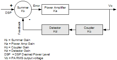
1. Introduction Power amplifier control (PAC) for a Global System for Mobile communications© (GSM©) compatible radio is one of the more challenging aspects of the GSM-based system design. Not only must the radio meet all output radio frequency (RF) spectrum specifications, but the Power Amplifier (PA) control loop must also be stable under varying environmental conditions. This paper starts by looking at the basic control theory, and discusses its advantages over simple open loop control. It then moves on to describe each block of the loop in detail. Stability is also discussed, and then finally, the paper examines a case study radio. 2. Power Amplifier Control Loop Figure 1 shows a typical PAC loop that uses proportional control. The control signal is proportional to the difference between the Detector/Coupler feedback and the DSP signal.
Figure 1. Typical PAC Loop with Proportional Control The first task is to find the transfer function for the Figure 1 loop, which can be done by noting the following relationships.
Simplifying:
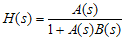
This expression, T, is commonly known as the closed loop gain. The product of gains, KaKsKdKc, is known as the loop gain. This control scheme is usually called proportional control, because the output voltage, Vo, is directly proportional to the error signal.
The closed loop gain is divided into a forward path gain “A” and a feedback path gain “B,” Figure 2. Substituting into the original equation produces the following more familiar output voltage expression:
where A = KaKs and B = KdKc.
Figure 2. Closed Loop Gain with Forward Path Gain A and Feedback Path Gain B 2.1 Benefits of Closed Loop Control In this section, the study compares open loop control, B = 0, to closed loop control. The advantages of closed loop control become apparent. 2.1.1 Temperature, Battery Insensitivity, and Linearization
If the loop gain remains >> 1 over temperature and battery ranges, then the output voltage, VO, becomes insensitive to temperature and battery effects. If AB >> 1, then the closed loop transfer function becomes:
Since KdKc is part of the feedback network and is usually a stable, temperature compensated block, there is a gain independence from battery supply and temperature. There is also a gain independence from KsKa variations when the radio environment differs from the one in which it was calibrated. Note. A radio's output power is calibrated during the manufacturing process to ensure compliance with GSM 11.10 output power requirements. 2.1.2 Sensitivity to Power Amplifier Gain Changes In general, the power amplifier (PA) gain, Ka is sensitive to both temperature and supply level. This can be stated mathematically as:
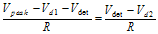
Since the design scheme is proportional control, there is a concern as to just how much the output power varies with a change in the PA gain. Assume Ks = 1 for the following calculations, that is, A = Ka, and starting with equation (2.8).
Writing this expression in incremental form yields the following:
To make this expression more useful, it can be written in terms of a fractional change of output voltage by dividing equation (2.12) by (2.8), which results in the following:
Now the relative change in output voltage vs. the change in PA gain is obvious. If the loop gain is >>1, then the gain change has very little effect on the output voltage change. But, as the loop gain changes from the calibration point, the change in output voltage becomes more and more sensitive to PA changes. For example, if the PA gain = 10%, and the loop gain = 100, how is the change in output power calculated? First, the fractional change in output power must be expressed in terms of voltage, which is the basic unit of loop operation. Again, Vo is an RMS voltage.
Hence, the output power, Po, changes by approximately 0.2%, or 0.009 dB.
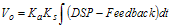
2.1.3 Loop Tracking Action Though it may not be obvious, the closed loop does in fact track the DSP signal. The best way to illustrate this is to look at the feedback signal. Once the system reaches steady state, the feedback signal should be nearly identical to the DSP signal.
Substituting the closed loop gain expression for Vo we have:
For a loop gain >> 1, the feedback signal can be observed that approximates the DSP signal. 2.2 Adding an Integrator to the Forward Path
Most PAC loops employ an integrator in the control loop forward path, Figure 3. This changes the topology from proportional control to integral control. As the previous section pointed out, the output power is a function of both the feedback gain, which is relatively stable, and the PA gain, which is sensitive to both temperature and supply, Ks =1. This is a problem when the loop gain is relatively low. Unfortunately, this low gain condition usually occurs at the highest system output power, where the tightest control is needed, per GSM 11.10, that is, for GSM Class 4, Power Level 5 (PL5).
Figure 3. PAC Loop with an Integrator in the Forward Path From Figure 3, it can be seen that the control voltage driving the PA is the integral of the error. In theory, integral control has the advantage that the loop settles to a point where the error is zero. Yet the integrator output provides the correct control voltage to the PA by integrating past errors. Re-writing the closed loop expression taking into account the integrator in the forward path provides insight as to what effect the integrator has on the steady operation of the loop.
Now differentiating wrt to time yields,
For
steady state, when
This is a design benefit. By using an integrator, the PA gain is essentially removed from loop steady state operations. In more practical terms, output voltage is expected to be the same even if the PA gain changes. This is intuitively obvious as the integrator drives the PA to the calibrated power level, so long as the feedback gain, KdKc, remains the same.
Although the integrator seems like an attractive solution, it does have a few drawbacks that the designer should be aware of. ● The loop now pushes the PA to get what it wants. If there are any conditions in which the PA cannot meet the calibrated output power, the loop drives the PA into saturation. This, in turn, can cause problems for switching transients.
● The integrator adds a phase shift/delay of 90° to the loop, so stability needs careful attention over all areas of operation. 3. PAC Loop Components
This section covers the following basic PAC loop components, see Figure 25, to include how they are commonly implemented: ● RF Detector ● Coupler 3.1 RF Detector The RF detector converts an output voltage scaled value into a DC voltage used for comparison with the DSP value. Given the detector is in the feedback loop, it is important that the detector is temperature compensated. Detector gain should also be stable over all operating conditions. Diode detector operation over one RF cycle is illustrated in Figure 4. From this, the average DC voltage; Vdet, can be derived. The graph indicates that the detector only works when the peak RF is greater than the diode “on” voltage. The voltage present at the detector input is defined as Vi = VoKc. Since this is a peak detector, the RMS value must be multiplied by to convert it to a peak voltage.
Figure 4. Diode Detector Operation over One RF Cycle To find the DC term, the Vdet voltage must be integrated over the range where it is greater than zero, as follows. First, the delay is calculated by realizing that the detector output is only active in the following case:
or
Now the delay, to, can be calculated:
Note. Equation 3.6 is only valid for cases in which equation 3.1 is true. Integrating from to to and multiplying by produces the DC term at the output:
If it is assumed that , and resulting integration is simplified, the following results:
For a Sinusoidal input, the detector gain can be derived to be:
If it is assumed that the input is a square wave and the same integration process is iterated, the results are:
Given the PA does not operate in a linear configuration, that is, GSM is a constant envelope, some non-linearity is expected. Hence, detector gain is bounded by –7 dB and –3 dB.
The following RF detectors are discussed below: ● Passive Single Diode Detector
● Temperature Compensated Passive Dual Diode Detector ● Active Temperature Compensated Dual Diode Detector 3.1.1 Passive Single Diode Detector
A diode detector functions as a simple half-wave rectifier. Its output voltage is nearly a linear function of the peak RF voltage applied. Since the detector operates at a high frequency, 900 MHz to 1800 MHz, it is important that the diodes used are capable of switching at this speed. The diode of choice has usually been the Schottky, given its ability to switch extremely fast. The Schottky also has a low Von voltage, typically around 200 mV, which helps to extend the lower range of the detector. Figure 5 shows a simple half-wave rectifier. The Rterm resistor is used to resistively match the detector, which gives a fairly flat response over frequency. The R and C form a filter that produces the DC detector voltage. The Schottky diode, as mentioned before, acts as a voltage-controlled switch that operates at RF. It is relatively easily to calculate a rough estimate for the lower end of the dynamic range, if all the data on the particular diode is available.
Figure 5. Diode Detector Functions as a Half-Wave Rectifier For example, suppose a diode has the following saturation current:
As long as the current through the diode is >> Is, the standard diode equation can be considered valid. For this example, Id is set = 45 nA, when the detector is at the lowest input range. It is also assumed that the detector can accurately operate down to an output of Vdet = 1 mV.
or
where K = Boltzmann's constant, T = Temperature in Kelvin, q = Magnitude of electronic charge At room temperature, Vt is approximately 25 mV. It should be apparent that the diode is a temperature-sensitive device, and, because it is in the feedback block, this problem needs to be addressed. Now the following expressions can be written:
Following the Section 3.1 integration process for square wave input.
Solving for R produces:
Solving for Vd, the diode drop at room temperature, produces:
and
Pmin, the minimum power, is 8.4 μW, or –20.7 dBm into 50 Ω.
3.1.2 Temperature Compensated Passive Dual Diode Detector In Section 3.1.1, although the passive single diode detector was capable of detecting RF, it had a temperature dependence. Since the detector is in the feedback loop, this is highly undesirable, and in some ways negates the use of negative feedback. If we introduce a second matched diode, as shown in Figure 6, we can, in principle, track out temperature changes.
Figure 6. Diode Detector with a Second Matched Diode To show the temperature compensation, the currents entering the Vdet node, see Figure 6, are summed:
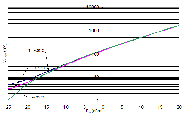
If Vd1 and Vd2 are matched, they track over temperature. As a practical note, the sensing circuitry at Vdet should not load this point down, because different currents run though the diodes and defeat the temperature compensation. Passive Dual Diode Detector performance analysis included measurements taken in the lab at 900 MHz over temperature, Figure 7. The detector is linear and well compensated at higher powers. Yet, at low temperatures, the detector is not compensated. The problem with lower temperatures is that Vd is higher, and it takes more power to turn on the diode(s). Effectively, the low temperature has limited the dynamic range. At room temperature, there is > 40 dB of dynamic range. Detector gain in V/V can be determined by looking at the slope of a line fit to the experimental data.
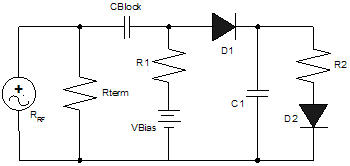
3.1.3 Active Temperature Compensated Dual Diode Detector Figure 8 shows an active diode detector schematic. This detector employs a slightly different principle than the passive single diode rectifying circuit. It is different because the diode, D1, is not turned off when the peak voltage is less than the VD1 drop, but charge is still deposited onto C1. When the RF voltage swings low, the charge on the capacitor C1 is not allowed to conduct back through D1. The net effect is a voltage increase across C1. The temperature compensation is not perfect, but it does remove the bulk of the shift due to temperature fluctuations. Some compensation can be observed by looking at the RF injection node at the anode of D1. Because this offset is dependent on temperature, the RF peak voltage also shifts with temperature. This change cancels the effects of the temperature dependent drop across D1. As the temperature increases, the drop across D1 decreases, and the current increases. This increase in current pulls the injection node down, thereby compensating for the lower drop across D1. Conversely, when the temperature drops, the current decreases, and the D1 drop increases. This decrease in current pulls the injection node higher, and again compensates for the larger D1 drop.
Figure 7. Passive Dual Diode Detector The quiescent bias point at Vdetect is temperature compensated, and can be shown using the same arguments as in Section 3.1.2. Active Dual Diode Detector performance analysis included detector performance over temperature, Figure 9. For this experiment, the diodes were biased at 50 mA, ensuring the diode is active over the entire range of operation. The active dual-diode detector has a major advantage over the passive dual-diode detector. Figure 7 and Figure 9 illustrate that at low temperatures, the active detector, Vdet, does not drop off like passive detector Vdet, Section 3.1.2. The active detector can operate quite well at –20 dBm to +20 dBm over the entire temperature range, giving it 40 dB of temperature compensated dynamic range.
Figure 8. Active Diode Detector Schematic
Figure 9. Active Dual Diode Detector 3.2 Coupler The coupler is a passive temperature stable device ideal for a feedback block. The coupler is important beyond the obvious connection to the feedback path. The amount of coupling defines not only dynamic range, but it also limits the minimum insertion loss in the output power path. Generally, couplers are found in the range of 10 dB to 20 dB, with the least amount of coupling being preferred for insertion loss. Coupler gain, Figure 10, is defined as
The amount of coupling also defines the amount of feedback gain, and ultimately limits the maximum amount of loop gain. Figure 10 coupling gain and insertion loss data is listed in Table 1.
Figure 10. Ideal Coupler Characteristics
Table 1. Coupling Gain and Insertion Loss
3.3 Error Computation The driving force behind any negative feedback system is error minimization. The error is represented by the difference between the requested DSP signal and the feedback signal magnitude. The next few sections cover a couple of different approaches to computing the error term. 3.3.1 Difference Amplifier
Error signal computation can be done using a difference amplifier shown in Figure 11.
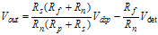
The output voltage is expressed as follows:
If we choose the resistors such that:
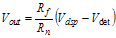
Figure 11. Difference Amplifier Circuitry Then Vout simplifies to:
The amplifier gain, , must be chosen so that the loop can achieve maximum power, and be able to produce a voltage low enough to shut the PA off. Vout_max is the worst-case maximum voltage to reach maximum power.
Assume Vdet_max is the worst-case output voltage at the highest power.
The DC offset could be non-zero, if an active detector is used. Amplifier output is
The minimum operable gain is:
Note. The DSP voltage should always be greater than the detector voltage at high power. The minimum output voltage is:
Vout_min < Minimum PA shut off voltage. The amp_gain maximum value follows:
The amp_gain expression follows:
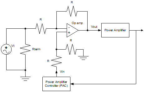
Hence, if the PA gain is too large, the PA cannot be shut off. If it is too low, maximum power cannot be achieved. If it is possible to make , the maximum gain limit is removed. 3.3.2 Differential Integrator The differential integrator is usually used in a PAC loop instead of a simple differential amplifier, Section 3.3.1. It is used to take advantage of an integrator in the forward path, discussed in Section 2.2. Figure 12 shows implementation using an operational amplifier.
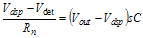
Figure 12. Implementation Using an Operational Amplifier Circuit analysis can be made using Laplace transforms. Summing the currents into the inverting node gives the following equation:
Solving for Vout:
Taking the inverse Laplace transform yields:
Note:
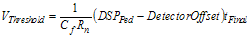
There are some limits to be considered. At maximum power the detector voltage should be less than the maximum DSP voltage, even in worst case. If it is not, then maximum power is not attainable. Also, the minimum Vdsp should be less than the Vdet with no RF applied, allowing the PA to be turned off. The Rn and Cf values are not arbitrary. For example, if there is certain amount of time to ramp up, integration must be fast enough, or there is time mask failure. On the other hand, if the integrator is too fast, there may be stability problems, or too much overshoot. Rn and Cf values are chosen by noting that the PA is off until the integrator output reaches threshold. While the output is less than the PA threshold, the loop is open. The following example shows how to calculate the integrator gain. The maximum time to close the loop follows:
Tlock = 8 μS (3.39) The Integrator differential voltage during pre-lock follows: Vdsp – Vdet = 15 mV (3.40)
The nominal PA Threshold voltage follows: Vo = 900 mV (3.41) Therefore, the differential integrator has 8 μS to integrate from 0 V to 900 mV with a 15 mV input.
Let
then
4. Loop Stability Loop stability is considered to be one of the most important criteria when designing a controller. Too much gain or too much lag can cause serious oscillatory problems. Looking at the closed loop gain expression again and making gains a function of frequency produces the following:
The loop gain becomes undefined at the point where T(s) = 1. At this particular operating point, loop oscillates. At the point where , loop gain is unity and has a phase of 180°. With respect to the loop gain, T(s), there are two figures of merit when specifying loop stability: ● Phase margin. The difference in the phase of T(s) and 180°, where the magnitude of T(s) = unity. ● Gain margin. The difference in the magnitude of T(s) and unity, where the phase of T(s) = 180°. Typically, the design target is a phase margin of 60° and gain margin of 10 dB. This covers temperature and component variations in the manufacturing process. 4.1 Measuring Gain and Phase Margin This section discusses the “small signal” method to measure loop stability. The small signal strategy is to inject a swept small signal into the loop and measure the effect of the loop on the swept signal.
In the loop in Figure 13, the summing node injects the test signal. To measure the loop gain, the transfer function for the parts of the summing unit that connect to the loop must be derived.
The error signal is written as
If the summing unit input is divided by the output:
which produces the loop gain shifted by 180°. Figure 14 shows a typical operational amplifier used as a summer circuit. The swept signal is fed into the inverting side, while the power controller output is fed into the non-inverting input. The operational amplifier output is then connected to the PA control port. A low frequency network analyzer, for example an HP 3577B, and a high impedance probe can be used to measure the transfer function from Vout to Vin. Caution: It is important to ensure the amplitude of the swept signal is kept relatively low so it does not effect the loop steady-state operation. It is also important for the op amp to have unity gain BW that is at least 10 times the loop BW that is being measured. Finally, the measurement device may not be able to sweep fast enough inside the GSM burst, so the PA may have to be run in continuous wave (CW) mode. This operational mode can limit the maximum power at which the loop response can be measured, because of thermal issues.
Figure 13. Loop Stability Using a Summing Node
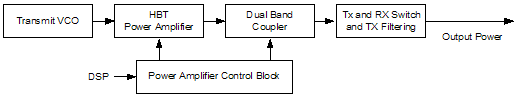
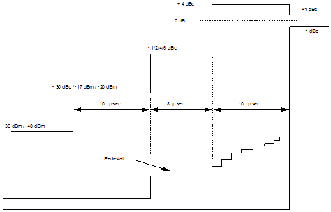
Figure 14. Operational Amp Used as a Summer 5. Case Study This section covers one of several GSM/DCS dual band handset design Figure 15 is this case study radio architecture block diagram. 5.1 Loop Building Blocks The following criteria, which are discussed below, are used in selecting the loop building blocks: ● Choosing a Coupler ● Forward Path Configuration 5.1.1 Choosing a Coupler Consider the following when choosing a dual band coupler: ● Insertion Loss ● Detector Dynamic Range ● Maximum output power of each band ● Minimum output power of each band ● Minimum detectable power (relates to Detector Dynamic Range) ● Difference between minimum power in each band Given Figure 15, it can be see that the PA output power is always greater than the radio output power. This difference in power is simply the insertion loss of the blocks in front of the PA. The insertion loss is 1.0 dB for GSM and 1.5 dB for DCS, assuming the coupler loss is negligible. The GSM-band radio is calibrated to +32 dBm for maximum power, not +33 dBm. ● GSM maximum power (PL5) = 32.0 dBm + 1.0 dBm = 33 dBm ● DCS maximum power (PL0) = 30.0 dBm + 1.5 dBm = 31.5 dBm. ● GSM minimum power (PL19) = 5 dBm + 1 dBm = 6 dBm ● DCS minimum power (PL15) = 0 dBm + 1.5 dBm = + 1.5 dBm The minimum power between the two bands has a 5 dB difference. If the coupling between bands is the same difference seen at the lowest power setup in both bands, pre ramp loop closure becomes band independent. The loop is locked to some small power pedestal prior to ramping. This pedestal ensures that the loop is locked and controllable prior to ramp up. The controllability ensures that there is a consistent ramp up in all radios Figure 16 illustrates this power pedestal and ramp timing. For the lowest power levels, GSM 11.10 relaxes the 6 dBc point to 1 dBc. In the case study, 4 dBc is targeted to produce a 3 dB margin. Given this information, the minimum detectable PA output power for both GSM and DCS can be determined. Using this data and the following definitions, and detecting minimum GSM output power to –20 dBm, GSM and DCS coupler values, equations (5.1) and (5.2), can also be determined. Pmin-det is the minimum detectable RF power in the detector Pmax-det is the maximum detectable RF power in the detector Pmin is the minimum PA output power
Figure 15. Radio Architecture Block Diagram
Figure 16. Power Pedestal Provides Loop Lock and Control Pmargin is the margin with respect to the 1 dBc point The safety margin is the part tolerance for the feedback loop circuitry in a mass volume environment. Pmax is the maximum PA output power Pmin is the minimum antenna output power + post-PA power loss
Where: GSM:
DCS:
Note. Minimum antenna output power is defined by GSM recommendation to be 5 dBm and 0 dBm for GSM and DCS respectively. This corresponds to PL19 and PL15 respectively.
where
For GSM:
For DCS:
The coupler's requirement is driven by minimum power out requirements as shown above. However, a check should be made to ensure that at high power, the detector is not over-driven.
As shown in Section 3.1.3 and Figure 9, the maximum detected RF power is sufficiently below the absolute detector RF power capability, which is at + 20 dBm. The preceding findings are summarized in Table 2.
Table 2. Case Study Findings
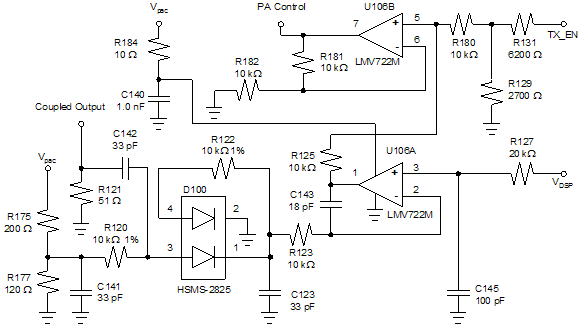
5.1.2 Forward Path Configuration This section discusses the forward control path configuration, which consists of: ● Difference amplifier. Combined with the integrator into one operational amplifier, the Differential Integrator block. ● Integrator. See above. ● DC offset function. Used to reduce the amount of variance in the time it takes to close the loop as explained below. In the test case, the Conexant CX77301, which has an APC threshold voltage of 1.0 V ± 200 mV, is used as the PA. Using the CX77301, the maximum offset used should be roughly 800 mV. The threshold is the bias point where the PA begins to conduct measurable current. This is also the control point where the PA begins to respond to inputs. Using this offset and appropriate integrator gain, the worst case time for closing the loop is about 8 μS. This is discussed Section 2.1. The error computation and integration circuitry is seen in Figure 17. An RC filter is added to the DSP control line to filter out any noise caused by the discrete steps produced by the digital-to-analog (D/A.) The RC is set to a corner of 80 KHz for the case study. The National Semiconductor LMV722 op amp is also used because of the following advantages: ● Reasonably high bandwidth, 10 MHz
● Operates rail to rail ● Consumes 8.4 mW of power ● Operates at the lower system supply voltage of 2.8 V ● Low noise level<
As shown in Section 3.3.2, the differential integrator circuitry, Figure 18, produces the integral of the difference of the applied signals in the case study. The offset block, summer amplifier circuitry, Figure 19, can also be achieved by using a resistor divider. Dividing down one of the system 2.8 V TX Enable signals produces the offset voltage. The PA control voltage is the sum of the integrator output and the desired offset. The offset voltage should be applied within the 28 μsec prior to bit0, so there is no possibility of failing the time mask requirements:
Note. Tx Enable is a binary signal total that enables the transmitter at 28 μsec before bit0 to 28 msec after bit147.
Figure 17. Forward Path Control Configuration
Figure 18. Differential Integrator Block Diagram
Figure 19. Summer Amplifier Circuitry 5.2 Design Challenges The most obvious design challenge is to satisfy GSM 11.10 requirements. The following two additional major challenges are discussed below:
● Pre-ramp loop closure ● Control loop stability 5.2.1 Pre-Ramp Loop Closure The power control loop should be in a closed state prior to ramp up. This closure ensures that the ramp up is consistent across production radios. For this particular challenge, the loop is considered closed once the PA reaches threshold. If there is any time left once the loop has the PA at threshold, the loop begins acquisition of the calibrated pedestal power level. Figure 20 shows the results at the integrator output if no offset is used. Because the PA is below threshold, there is no PA output power produced, and the detector voltage remains constant. The net effect is that the integrator simply operates on a constant, producing a linear response. A general approximation for the time needed to close the loop follows:
Where and are integrator components. The loop close time is dependent on the following variables: ● Vthreshold, which is applied to the PA control port
● DSP D/A PA threshold variation is out of the designers' control. The best that can be done is to ensure the loop works under all threshold ranges. The DSP signal is the result of calibration and its magnitude reflects the amount of system coupling. Because perfect couplers cannot be manufactured, some variations in coupling exist between like parts. If the coupling is light, then DSP is smaller than nominal, if the coupling is heavier, the DSP signal tends to be larger than nominal.
Figure 20. Integrator Output Timing Diagram 5.2.1.1 Closure with Zero Offset The following is known when closing the loop with a zero volt offset at integrator output: ● Coupler Variance = ± 1 dB
● Vthreshold Range = 1.0 V ± 200 mV For both GSM and DCS, input power applied to the detector equals 17 dBm ±1dB. Detected voltage data for the GSM and DCS bands is shown in Table 3 and Table 4 respectively.
Table 3. GSM Detected Voltage Data
Table 4. DCS Detected Voltage Data
Since GSM has the lowest output of 12.6 mV, it should be used as the worst case DSP input for slowest lock time. From the previous timing diagram in section 5.1.1, the loop has to reach threshold within 8 μS. Knowing this, the gain needed at the integrator stage can be calculated. Seven μS is used to ensure closure before 8 μS.
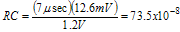
Letting R = 10 kΩ, C = 7.35 pF. In this case study, these values were tried. Although the loop closed in time, it was unstable in some regions of operation. A new approach was needed to solve this problem. 5.2.1.2 Closure with a Fixed Integrator Offset
A fixed offset applied at the integrator output allows the loop to operate at a lower and more stable gain. If the offset is set to 700 mV, then the maximum integrator output becomes (1.2 V) – (0.8 V) = 500 mV. Using this new 500 mV maximum threshold and a maximum closure period of 8 μsec, the new required gain can be calculated. Again 7 μsec is used to ensure closure before the 8 μS limit. The 12.6 mV comes from the previous section.
Letting R = 10 kΩ, C = 18 pF. Using these new values in the case study radio produced a stable loop that easily closed prior to the 8 μsec limit. Results
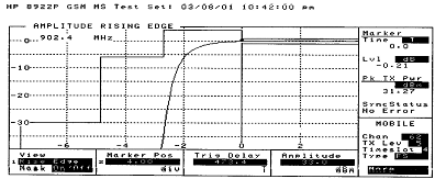
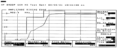
Figure 21 is GSM channel 62 ramp up for high power. Figure 22 is GSM channel 62 ramp up for low power.
Figure 21. GSM Channel 62 Ramp Up for High Power
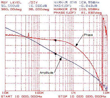
Figure 22. GSM Channel 62 Ramp Up for Low Power 5.2.2 Stability Using the C = 18 pF integrator capacitor and R = 10 kΩ resistor, loop stability was measured. The set up used was exactly as described in Section 4, Figure 23 shows a typical loop response followed by a set of condensed phase and amplitude measurements. In this particular plot, phase margin is 61 degrees and gain margin is about 20 dB. The loop bandwidth is roughly 276 kHz. Table 5 and Table 6 include the tabulated results of lab measurements at different power levels for the GSM and DCS bands respectively. Taking the measurement in CW mode limits the maximum power at which the measurement can be made. The low frequency gain, Ao, is given at 10 kHz. When the loop is operating near +24.0 dBm in DCS mode, it can be seen that the gain margin is severely compromised. Although no oscillations were found in the lab under various conditions, the designer should be aware of this potential problem that would show up as a sideband at 2.6 MHz. For the case study, time restrictions precluded going back to compensate the loop.
Figure 23. Typical Loop Response and Condensed Measurements
Table 5. Results of Lab Measurements at Different GSM Power Levels
Table 6. Results of Lab Measurements at Different DCS Power Levels
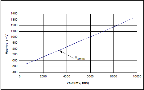
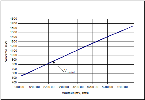
5.3 Control Characteristics Figure 24 shows basic GSM control characteristics plots, VDSP vs. VOUT. Figure 25 shows basic DCS control characteristics plots, VDSP vs. VOUT. The slope of the control curves is equal to the gain of the feedback block, given the steady state condition of Vdetector = VDSP. The GSM plot has a slope of about 12.5 or 22 dB, this is close to what is expected given a 19 dB coupler and a detector with – 3dB of gain. The DCS plot has a slope of 7 or 17 dB, this also follows because of the 14 dB coupler used, and the detector gain is again about 3 dB. The most important point in these measurements is that the detector appears to be linear over the operational range. 5.4 Discrete Power Controller
Schematic Figure 26 shows the case study radio schematic. VPAC is 2.8 V and TX_EN is a 2.8 V transmit control signal that is enabled 20 μsec prior to bit zero.
6. Conclusion This paper examined basic control loop theory and presented technical detail for each block in the loop. It also included some of the challenges involved in designing a power amplifier control loop. After briefly reviewing each block, the paper discussed loop stability and how to measure it. A case study radio was presented that was designed using the concepts covered in this paper. The case study radio operated well within GSM 11.10 requirements and had a stable control loop. References
Analysis and Design of Analog Integrated Circuits Grey, Paul R.; Robert G. Meyer.
New York: John Wiley & Sons Inc., 1993 Feedback Control of Dynamic Systems
Franklin, Gene F.; J. David Powell; Abbas Emami-Naeini Reading: Addison-Wesley Publishing Company, 1991
About the Author Jason Millard received his BSEE degree from University of Illinois, Champaign-Urbana in 1994. He joined Motorola subscriber division in 1995, in Libertyville, Illinois where he developed GSM cellular handsets. In 1998 he joined wireless communication division of Conexant systems Inc where his development of GSM cellular systems continues as a senior staff engineer. Darioush Agahi, P.E. is director of GSM RF systems engineering at Conexant Systems Inc. in Newport Beach CA. Prior him joining Conexant in 1996 he worked for nine years for Motorola's (GSM) cellular subscriber division. Darioush received his BS in electronics (1981) and MS in Medical Engineering from the George Washington University in Washington DC (1983). Also he received an MSEE from Illinois Institute of Technology in Chicago Illinois (1993) and an MBA from National University in 1997. Darioush holds twenty one US patents plus he is a Professional Engineer (P.E.) registered in the state of Wisconsin.
Figure 23. GSM Discrete PAC Control Characteristics (VDSP vs. VOUT)
Figure 24. DCS Discrete PAC Control Characteristics (VDSP vs. VOUT)
Figure 25. Case Study Radio Schematic
|
|||||||||||||||||||||||||||||||||||||||||||||||||||||||||||||||||||||||||||||||||||||||||||||||||||||||||||||||||||||||||||||||||||||||||||||||||||||||||||||||||||||||||||||||||||||||||||||||||||||||||||||||||||||||||||||||||||||||||||||||||||||||||||||||||||||||||||||||||||||||||||||||||||||||||||
 (2.1)
(2.1)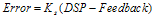 (2.2)
(2.2) (2.3)
(2.3)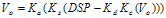 (2.4)
(2.4)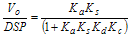 (2.5)
(2.5)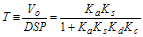 (2.6)
(2.6)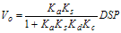 (2.7)
(2.7) (2.8)
(2.8)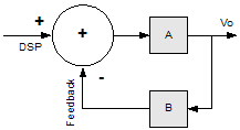
 (2.9)
(2.9)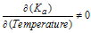 , and (2.10)
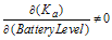 (2.11)
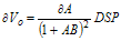 (2.12)
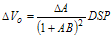 (2.13)
 (2.14)
 (2.15)
 (2.16)
 (2.17)
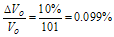 (2.18)
 (2.19)
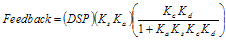 (2.20)
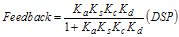 (2.21)
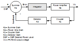
 (2.22)
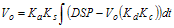 (2.23)
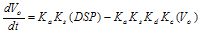 (2.24)
 , we have
 (2.25)
 (2.26)
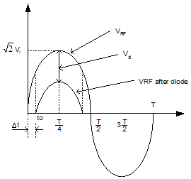
 (3.1)
(3.1) (3.2)
(3.2) (3.3)
(3.3)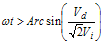 (3.4)
(3.4) (3.5)
(3.5)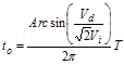 (3.6)
(3.6)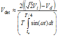 (3.7)
(3.7) , Sine wave input
(3.8)
, Sine wave input
(3.8)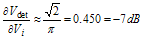 (3.9)
(3.9)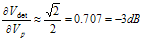 (3.10)
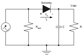
 (3.11)
 (3.12)
 (3.13)
 (3.14)
 (3.15)
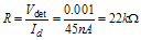 (3.16)
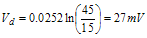 (3.17)
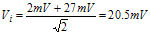 (3.18)
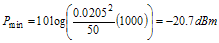 (3.19)
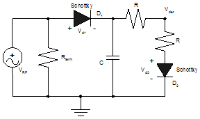
 (3.20)
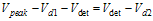 (3.21)
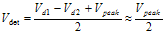 (3.22)
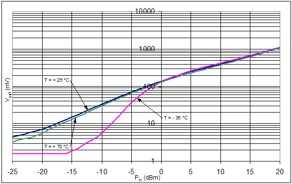
 (3.23)
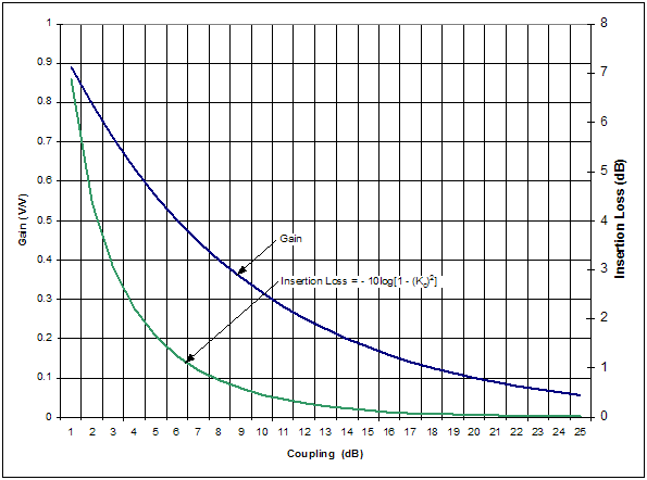
 (3.24)
 (3.25)
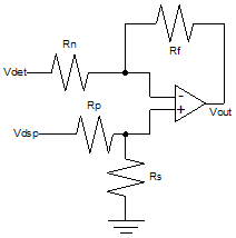
 (3.26)
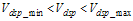 (3.27)
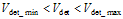 (3.28)
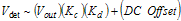 (3.29)
 (3.30)
 (3.31)
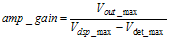 (3.32)
 (3.33)
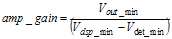 (3.34)
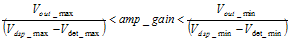 (3.35)
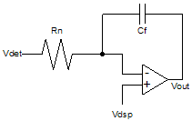
 (3.36)
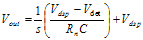 (3.37)
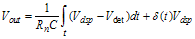 (3.38)
 multiplies with the
integral difference, which is the differential integrator effective gain.
multiplies with the
integral difference, which is the differential integrator effective gain.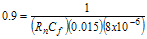 (3.42)
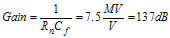 (3.43)
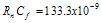 (3.44)
 ,
,
 (4.1)
(4.1)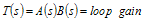 (4.2)
(4.2) (4.3)
(4.3) ,
(4.4)
,
(4.4)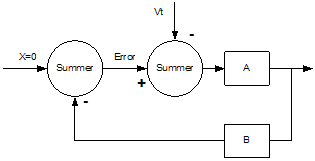
 (5.1)
(5.1) (5.2)
(5.2)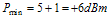 (5.3)
(5.3)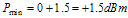 (5.4)
(5.4)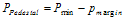 (5.5)
(5.5)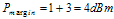 (5.6)
(5.6)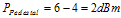 (5.7)
(5.7) (5.8)
(5.8) (5.9)
(5.9) , at its output
 (5.10)
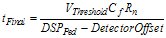 (5.11)
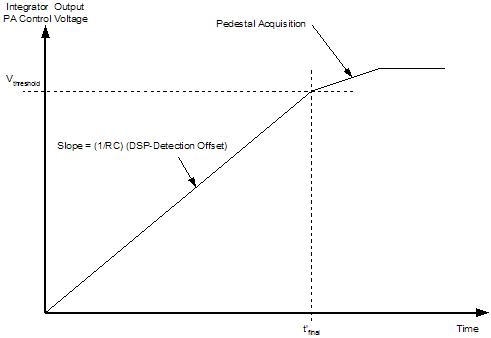
 (5.12)
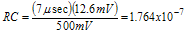 (5.13)