| Electronics & High Technology Components |
|
Rather than always linking to Wikipedia entries for common topics, I have been using ChatGPT to research and post brief summaries on many technical topics. The results are not always perfect, but I edit them as needed to be accurate. Courts have ruled that AI-generated content is not subject to copyright restrictions, but since I modify them, everything here is protected by RF Cafe copyright. Here are the major categories. Electronics & High Technology Company History | Electronics & Technical Magazines | Electronics & Technology Pioneers History | Electronics & Technology Principles | Technology Standards Groups & Industry Associations | Vintage Vacuum Tube Radio Company History | Electronics & High Technology Components | Societal Influences on Technology | Science & Engineering Instruments Companies
Autodyne Receiver An autodyne receiver is a type of radio frequency (RF) receiver that uses a local oscillator to mix with the incoming RF signal for the purpose of down-conversion. It is also known as a self-oscillating mixer or a self-mixing receiver. In a traditional superheterodyne receiver, a separate local oscillator generates a stable frequency that is mixed with the incoming RF signal to produce an intermediate frequency (IF). However, in an autodyne receiver, the local oscillator signal is derived from the incoming RF signal itself. This self-oscillation is achieved by feeding back a portion of the RF signal into the oscillator circuit. The autodyne receiver's oscillator generates a frequency close to the RF frequency of the incoming signal. When the RF and local oscillator signals mix, they produce a frequency that is the difference between the two. This frequency is typically the desired intermediate frequency. Autodyne receivers are used in various applications, including radio communication, radar systems, and electronic warfare. They offer advantages such as simplicity, lower cost, and reduced complexity compared to separate local oscillator designs. However, they can be more susceptible to spurious oscillations and require careful design to achieve stable operation. - See Full List - Capacitors, Polystyrene Polystyrene is a type of plastic that has been widely used as a dielectric material in capacitors. Dielectric materials are used to separate the conductive plates of a capacitor and enhance its electrical properties. Here's some information about polystyrene as a dielectric material in capacitors, including its frequency response, quality factor, voltage breakdown, capacitance, and a brief history. Frequency Response: Polystyrene capacitors exhibit excellent frequency response characteristics. They have low loss and can maintain stable capacitance values over a wide range of frequencies, making them suitable for applications requiring high-frequency stability. Quality Factor (Q): The quality factor, or Q factor, represents the energy storage and loss characteristics of a capacitor. Polystyrene capacitors typically have high-quality factors, indicating low energy losses and efficient energy storage. This makes them suitable for applications requiring high Q factors, such as resonant circuits and filters. Voltage Breakdown: Polystyrene capacitors generally have a high voltage breakdown rating, allowing them to withstand relatively high voltage levels without suffering from electrical breakdown. This feature makes them suitable for applications requiring high voltage handling capabilities. Capacitance: The capacitance of polystyrene capacitors is determined by the physical dimensions of the capacitor, the dielectric constant of polystyrene, and the dielectric thickness. Capacitance values for polystyrene capacitors can range from picofarads (pF) to a few microfarads (µF). Polystyrene capacitors are known for their stability, low tolerance, and low temperature coefficient of capacitance. History: Polystyrene capacitors have been used since the early 20th century. They gained popularity for their excellent electrical properties, including high stability, low loss, and low dielectric absorption. Polystyrene capacitors were commonly used in applications such as audio equipment, precision measurement devices, and high-frequency circuits. However, over time, other dielectric materials like polypropylene, polyester, and ceramic capacitors became more prevalent due to cost, size, and manufacturing advantages. It's worth noting that while polystyrene capacitors offer excellent electrical characteristics, they are relatively large in size compared to modern capacitor technologies. As a result, their usage has become less common in recent years, with other smaller and more cost-effective dielectric materials dominating the market. - See Full List - Coherer The coherer, developed by French physicist Édouard Branly in the late 19th century, is a type of early radio wave detector. It consists of a glass tube filled with metal filings or metal powders, typically iron. The filings or powders form loose contacts, allowing the device to be highly sensitive to electromagnetic waves. When radio waves pass through the coherer, the metal particles inside would coalesce or stick together, causing a decrease in electrical resistance. This change in resistance could then be detected and used to indicate the presence of radio waves. Sir Oliver Joseph Lodge is believed by some people to be the inventor of the coherer. - See Full List - Cold Cathode Vacuum Tube A cold cathode vacuum tube, also known as a cold cathode tube or simply a cold tube, is a type of vacuum tube that does not require a heated filament to emit electrons. Instead, it uses a cathode that is made of a material with a low work function, such as certain metals or semiconductors. When a high voltage is applied between the anode and the cathode, electrons are emitted from the cathode and flow toward the anode. The absence of a heated filament distinguishes cold cathode tubes from hot cathode tubes, such as the more common vacuum tubes like the triode or the tetrode. In a hot cathode tube, the filament is heated to a high temperature, which causes electron emission. Cold cathode tubes can be found in various applications, such as neon lights, voltage regulators, and gas discharge tubes. They are also used in some types of vacuum fluorescent displays (VFDs), where they provide bright and uniform illumination. One specific example of a cold cathode vacuum tube is the Nixie tube. Nixie tubes were popular in the mid-20th century as numeric displays for electronic devices like calculators, counters, and clocks. They consist of a series of cathodes in the shape of numerals or other symbols, surrounded by a mesh anode. When a specific cathode is activated by applying voltage to it, the corresponding numeral or symbol lights up. Overall, cold cathode vacuum tubes offer an alternative method of electron emission compared to hot cathode tubes and have found applications in various electronic devices. - See Full List -
Computer punched cards were a popular data storage and input medium in early computer systems. Punched cards were widely used from the 1920s through the 1970s and played a significant role in the development of computing. Computer punched cards were made of stiff cardstock and had rectangular holes punched in specific positions. These holes represented data and instructions that could be processed by machines called card readers or tabulating machines. The most common type of computer punched card had dimensions of 7.375 inches by 3.25 inches (187.33 mm by 82.55 mm) and featured 80 columns and typically 12 rows of holes. Each column could hold a character or a specific piece of information. The absence or presence of a hole in a particular column indicated specific data or instructions. Programs, data, and instructions were encoded onto the punched cards using keypunch machines. Operators would use the keypunch machines to punch holes in the appropriate columns and rows to represent the desired information. Computer punched cards were used for various purposes, including data entry, data storage, and batch processing. They allowed for the input and storage of large amounts of data, such as census information, scientific data, business records, and more. Programs and instructions were also stored on punched cards, allowing for sequential execution in batch processing systems. As technology advanced, punched cards were gradually replaced by more efficient and versatile storage and input methods, such as magnetic tape, magnetic disk, and eventually electronic storage. Today, punched cards are considered obsolete, and their usage has been largely phased out in favor of modern computer systems and storage media. Here is a comprehensive review of various computer punched card encoding / decoding schemes. - See Full List -
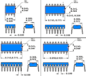
A Dual Inline Package (DIP) is a type of electronic component packaging used for integrated circuits (ICs) and other electronic devices. DIPs were widely used in the electronics industry for several decades, but they have largely been replaced by surface-mount technology (SMT) packages in recent years. Here's a brief history of the DIP:
- See Full List -
Gallium arsenide (GaAs) is a member of the III-V group of compound semiconductors, which includes materials made from a combination of elements from the third and fifth groups of the periodic table, such as gallium, indium, and aluminum with nitrogen, phosphorous, or arsenic. III-V semiconductors have unique properties that make them useful for a wide range of electronic and optoelectronic applications. For example, they have high electron mobility, high thermal conductivity, and direct bandgaps, making them ideal for use in high-speed electronic devices, LEDs, solar cells, and other optoelectronic devices. In addition to GaAs, other commonly used III-V semiconductors include indium phosphide (InP), aluminum gallium arsenide (AlGaAs), and indium gallium arsenide (InGaAs). These materials are used in a variety of applications, such as wireless communication devices, fiber-optic networks, high-efficiency solar cells, and solid-state lighting. Overall, III-V semiconductors are essential materials in modern electronics and are used to create many of the devices that power our daily lives. - See Full List - Gallium Nitride (GaN) Semiconductor Gallium nitride (GaN) is a binary III-V compound semiconductor composed of gallium (Ga) and nitrogen (N). It is a wide-bandgap material with unique electrical and optical properties that make it suitable for a variety of applications, including high-frequency and high-power electronic devices, light-emitting diodes (LEDs), and laser diodes. GaN is typically grown as a thin film on a substrate, such as sapphire or silicon carbide, using various methods such as molecular beam epitaxy (MBE) and metal-organic chemical vapor deposition (MOCVD). The resulting GaN film can then be patterned and etched to create devices such as transistors, diodes, and LEDs. One of the key advantages of GaN is its high electron mobility, which allows for high-frequency operation and efficient power conversion. GaN devices can also operate at higher temperatures than traditional silicon-based devices, making them suitable for use in high-temperature environments. Additionally, GaN has a higher breakdown voltage than other materials, making it suitable for use in high-voltage power electronics. GaN-based LEDs have several advantages over traditional incandescent and fluorescent lighting, including higher efficiency, longer lifetime, and improved color rendering. GaN-based laser diodes are used in a variety of applications, including Blu-ray disc players, laser printers, and fiber-optic communication systems. - See Full List - Germanium (Ge) Semiconductor Germanium (Ge) is another semiconductor material that was widely used in early electronics, before being largely replaced by silicon. Germanium is a metalloid, similar to silicon, and has properties that make it suitable for use in electronic devices. Germanium has a higher electron mobility than silicon, which makes it attractive for use in high-speed transistors and other electronic devices. However, it has a lower thermal conductivity and a smaller bandgap than silicon, which limits its use in some applications. Germanium is still used in some niche applications, such as in infrared detectors and nuclear radiation detectors, where its unique properties make it useful. It is also being researched for potential use in solar cells and other electronic devices, as scientists continue to explore new materials and technologies. While germanium is not as widely used as it once was, it remains an important material in the electronics industry and continues to be studied for its potential uses. - See Full List -
A manpack radio, also known as a backpack radio or portable military radio, is a communication device designed to be carried and operated by an individual soldier or small team. It is typically used for military purposes but can also be employed in other fields such as emergency services or outdoor activities. Manpack radios are designed to provide reliable and secure communication in the field, allowing soldiers to communicate with each other, their command centers, and other units. These radios are typically ruggedized and built to withstand harsh environments, including extreme temperatures, moisture, dust, and shock. Some key features of manpack radios may include: Portability: Manpack radios are designed to be compact and lightweight, allowing soldiers to carry them on their person or in a backpack. Frequency Range: They can operate across a wide frequency range, including HF (High Frequency), VHF (Very High Frequency), and UHF (Ultra High Frequency), depending on the specific model. Encryption: Many manpack radios support encryption capabilities to ensure secure communication, preventing unauthorized access to sensitive information. Long Range: Manpack radios often have extended communication ranges, allowing soldiers to communicate over considerable distances, even in remote or difficult terrain. Power Source: They typically have built-in batteries or can be powered by rechargeable batteries, providing extended operational time. Some models may also have options for external power sources or solar charging. Durability: Manpack radios are designed to withstand rough handling and environmental conditions encountered in military operations. They are often water-resistant or even waterproof and can withstand vibrations, shocks, and drops. Voice and Data Communication: Manpack radios support both voice and data transmission, allowing soldiers to exchange information, send reports, and share coordinates or other critical data. - See Full List -
Methyl chloroform, also known as 1,1,1-trichloroethane, is a chemical compound with the molecular formula CH3CCl3. It is a chlorinated hydrocarbon and was historically used as a solvent and cleaning agent. However, it has largely been phased out and replaced by less environmentally harmful solvents due to its contribution to ozone depletion and its potential health hazards. Methyl chloroform was once widely used in various industrial applications, including as a degreasing agent and in the production of aerosol propellants and refrigerants. However, its use has declined significantly due to environmental concerns. The compound is known to be an ozone-depleting substance, meaning that it can release chlorine atoms when it breaks down in the atmosphere. These chlorine atoms can then contribute to the destruction of ozone molecules in the stratosphere, leading to the depletion of the ozone layer. Due to its adverse environmental impact and health risks associated with its use, many countries have implemented regulations and restrictions on the production and use of methyl chloroform. The Montreal Protocol, an international treaty, has also called for the phase-out of methyl chloroform and other ozone-depleting substances to protect the Earth's ozone layer. As a result, its production and use have been largely replaced by alternative solvents and chemicals. - See Full List - Primary Battery A primary battery, also known as a disposable battery, is a type of electrochemical cell that generates electrical energy through a one-time chemical reaction. Unlike secondary batteries (rechargeable batteries), primary batteries cannot be recharged or reused after they have been depleted. Once the chemical reactions inside a primary battery have run their course, the battery is no longer capable of producing electricity and must be discarded. Here are some key characteristics and features of primary batteries: Single Use: Primary batteries are designed for single-use applications. Once their energy is depleted, they are typically discarded, and new batteries must be installed. Convenience: Primary batteries are convenient for devices that have low power demands or devices that are used infrequently because they come pre-charged and are ready for immediate use. Self-Contained: Primary batteries are self-contained units, meaning they do not require an external power source or charging equipment to operate. This makes them suitable for a wide range of portable devices. Various Chemistries: There are different types of primary batteries available, each with its own chemistry and characteristics. Common types include alkaline batteries, zinc-carbon batteries, lithium batteries, and silver oxide batteries, among others. Limited Lifespan: Primary batteries have a limited lifespan based on the capacity of the chemical reactions occurring within them. Their lifespan depends on factors such as the type of battery, its capacity, and the power demands of the device it's used in. Common Applications: Primary batteries are used in various consumer electronics and devices, such as remote controls, flashlights, smoke detectors, toys, and some medical devices. Environmental Considerations: Due to their single-use nature, primary batteries can contribute to electronic waste (e-waste) when not disposed of properly. Some types of primary batteries contain hazardous materials, such as mercury or cadmium, which can be harmful to the environment if not recycled or disposed of according to regulations. - See Full List - Secondary Battery A secondary battery, also known as a rechargeable battery or storage battery, is a type of electrochemical cell that can be charged and discharged multiple times through reversible chemical reactions. Unlike primary batteries, which are designed for single use and cannot be recharged, secondary batteries are designed for multiple charge and discharge cycles, making them a more sustainable and cost-effective choice in the long run. Here are some key characteristics and advantages of secondary batteries: Rechargeable: The primary advantage of secondary batteries is their ability to be recharged. They can be connected to an external power source, such as a charger, to replenish their energy and be reused multiple times. Environmental Benefits: Secondary batteries are more environmentally friendly compared to primary batteries because they reduce the number of disposable batteries that end up in landfills. This helps reduce the environmental impact of battery waste. Cost-Efficient: While secondary batteries may have a higher upfront cost than primary batteries, they can be more cost-effective in the long term because they can be recharged and reused many times. Variety of Chemistries: There are various types of secondary batteries, each with its own chemistry and characteristics. Common types include lithium-ion (Li-ion), nickel-metal hydride (NiMH), lead-acid, and nickel-cadmium (NiCd) batteries. These batteries have different energy densities, discharge rates, and cycle life characteristics, making them suitable for different applications. Applications: Secondary batteries are used in a wide range of applications, including portable electronics (e.g., laptops, smartphones, and digital cameras), electric vehicles (EVs), renewable energy storage (e.g., solar power systems), uninterruptible power supplies (UPS), and more. Energy Storage: Secondary batteries play a crucial role in energy storage systems, helping store excess energy generated from renewable sources like solar and wind for use when needed. Maintenance: Secondary batteries require some maintenance, such as periodic charging and proper storage to maximize their lifespan and performance. - See Full List -
A selenium rectifier is a type of rectifier that uses selenium as a semiconductor material to convert alternating current (AC) to direct current (DC). Selenium rectifiers were commonly used in electronics applications during the mid-20th century, but they have since been largely replaced by other types of rectifiers such as silicon rectifiers. A selenium rectifier element refers to the selenium wafer or disc used as the rectifying material in a selenium rectifier. The element typically consists of a cylindrical or disc-shaped piece of selenium that is sandwiched between two metal plates or electrodes. When an AC voltage is applied across the electrodes, the selenium element acts as a semiconductor and allows current to flow in only one direction, effectively rectifying the AC signal into a DC signal. Selenium rectifiers have several advantages over other rectifier types, such as high reliability, long lifespan, and low cost. However, they also have some drawbacks, including relatively low efficiency and the potential release of toxic selenium compounds when the rectifier is heated or damaged. As a result, selenium rectifiers are now mostly obsolete and have been replaced by more efficient and safer rectifier technologies. Selenium is a chemical element with the atomic number 34, and it is a non-metal in the periodic table. Here are some of the properties of selenium: Physical properties: Selenium is a grayish-black, brittle solid at room temperature, with a metallic luster. It has a melting point of 217 degrees Celsius and a boiling point of 684 degrees Celsius. Chemical properties: Selenium is a relatively reactive element that readily combines with other elements to form compounds. It is also a good conductor of electricity and can act as a semiconductor when doped with impurities. Selenium is found naturally in the Earth's crust, often in association with sulfur, and it is widely distributed in rocks, soils, and water. It is also a byproduct of the refining of certain metals, such as copper and lead. To process selenium for use in electronic components, such as rectifiers, the element is first extracted from its ores and purified through a series of chemical and physical processes. The resulting purified selenium is then shaped into the desired form, such as wafers or discs, and assembled into the rectifier components. There are some potential dangers associated with selenium, especially when it is in its elemental form. Exposure to high levels of selenium can cause a range of health effects, including respiratory irritation, gastrointestinal disturbances, and neurological symptoms. Selenium can also be toxic to aquatic life and can accumulate in the food chain, so proper handling and disposal of selenium-containing materials are important to minimize environmental impacts. Despite the potential risks associated with selenium, it has a variety of important industrial and technological uses. In addition to its use in rectifiers, selenium is used in photovoltaic cells, glassmaking, pigments, and animal feed supplements. It is also a trace element that is essential to human health in small amounts. - See Full List - Semiconductor Boule A semiconductor boule is a large, single crystal ingot of semiconductor material, usually silicon, that is produced using the Czochralski method. During this process, high-purity silicon is melted in a crucible, and a seed crystal is slowly pulled out of the molten material while the crucible rotates. As the crystal is pulled out, it solidifies into a cylindrical ingot, which can be several feet in length and several inches in diameter. The resulting boule's properties, such as crystal structure and electrical characteristics, can be carefully controlled during the growth process to ensure that the resulting wafers have the desired properties. It's worth noting that the quality of the boule is critical to the performance of the semiconductor devices that are made from it, as even small defects or impurities can affect the electrical behavior of the material. After the boule is produced, it is sliced into thin wafers, which are used as the foundation for manufacturing semiconductor devices. Semiconductor boules are an essential component of the electronics industry and play a crucial role in producing many of the devices that we use in our daily lives. - See Full List - Silicon (Si) Semiconductor Silicon is widely used as a semiconductor substrate in the electronics industry. A semiconductor substrate is a material upon which electronic devices, such as transistors and integrated circuits, are built. The properties of silicon make it an ideal substrate for semiconductor devices. Silicon is a widely available material, it is relatively inexpensive, and it can be easily purified to high levels of purity. It also has a high melting point, good thermal conductivity, and favorable electrical properties that make it an excellent semiconductor material. When silicon is doped with small amounts of other elements, such as boron or phosphorus, it can be transformed into p-type or n-type semiconductors, respectively. These different types of semiconductors have different electrical properties that can be harnessed to create a wide range of electronic devices. Overall, silicon is a crucial material in the electronics industry, serving as the foundation for many of the devices that power modern technology. - See Full List - Superconductor The history of superconductors spans over a century and has led to significant advancements in the field of physics and technology. A superconductor is a material that exhibits zero electrical resistance and the expulsion of magnetic fields when it is cooled below a critical temperature. In other words, it can conduct electric current without any loss of energy due to resistance, and it can also expel magnetic fields from its interior. This phenomenon is known as superconductivity. Superconductors have numerous practical applications, including in the construction of powerful magnets for medical devices like MRI machines, high-speed electronic circuits, and potentially even in energy transmission and storage systems. Superconductivity is a quantum mechanical phenomenon that was first discovered in certain metals and has since been observed in various materials, including ceramics and some specialized compounds. Discovery of Superconductivity (1911): Superconductivity was first discovered by Heike Kamerlingh Onnes, a Dutch physicist, in 1911. He was conducting experiments to liquefy helium when he observed that the electrical resistance of mercury dropped to zero at temperatures below 4.2 Kelvin (-268.95°C or -452.11°F). Early Discoveries and Research (1911-1930s): Researchers like John Bardeen, Leon Cooper, and Robert Schrieffer developed the BCS theory of superconductivity in 1957, which explained the behavior of conventional (low-temperature) superconductors. This theory is still widely accepted today. During this time, several superconducting materials were discovered, including lead, niobium, and tin. Liquid Helium Era (1950s-1960s): The early era of superconductivity research mainly focused on low-temperature superconductors that required liquid helium for cooling. This limited their practical applications due to the high cost and difficulty of maintaining such low temperatures. High-Temperature Superconductors (1986): A major breakthrough came in 1986 when IBM researchers Georg Bednorz and K. Alex Müller discovered a new class of superconductors that exhibited superconductivity at significantly higher temperatures. Their discovery involved copper oxides, specifically La-Ba-Cu-O compounds, which became known as "high-temperature superconductors." These materials could operate at temperatures above the boiling point of liquid nitrogen (-196°C or -321°F), making them more practical for various applications. Further Research and Applications: High-temperature superconductors sparked intense research, leading to the discovery of various other families of materials with similar properties. Superconductors found applications in various fields, including medical imaging (MRI machines), particle accelerators, power transmission, and more. Researchers continued to work on increasing the critical temperatures (Tc) of superconductors, as well as developing practical methods for producing and using them. Iron-Based Superconductors: In 2008, a new class of superconductors called "iron-based superconductors" was discovered. These materials also exhibit superconductivity at relatively high temperatures, although not as high as some high-temperature cuprate superconductors. - See Full List -
Thyristor is a type of semiconductor device that is widely used in power control applications. It is also known as a Silicon Controlled Rectifier (SCR). Here is some information about its invention, inventor, uses, construction, fabrication, and schematic symbol: Invention and Inventor: The thyristor was invented by William Shockley, John Bardeen, and Walter Brattain in 1947 while they were working at Bell Laboratories. They were awarded the Nobel Prize in Physics in 1956 for their invention of the transistor, which is a related device. Uses: Thyristors are used in a variety of applications that require precise control of electrical power. Some common uses include motor control, lighting control, temperature control, and power conversion. Construction and Fabrication: A thyristor is a four-layer semiconductor device that consists of two PN junctions, with an additional P or N layer between them. The device is made of silicon, and it is manufactured using a process similar to that used to make transistors. The construction of the thyristor allows it to be turned on and off by applying a small signal to the gate terminal. Schematic Symbol: The schematic symbol for a thyristor consists of two P-N junctions connected in series, with a gate terminal at the junction between the P and N layers. The symbol is similar to that of a diode, but with an additional terminal for the gate. - See Full List - Tokomak A tokamak is a device used to confine and control plasma in order to achieve controlled nuclear fusion. It is one of the most promising approaches to achieving practical fusion energy. The word "tokamak" is derived from the Russian acronym for "toroidal chamber with magnetic coils." The basic design of a tokamak involves a donut-shaped vacuum chamber surrounded by magnetic coils. The plasma, which is a hot, ionized gas, is injected into the chamber and heated to extremely high temperatures using various heating methods such as radiofrequency waves or neutral beam injection. The magnetic coils produce a strong magnetic field that shapes and confines the plasma within the donut-shaped chamber. This magnetic confinement prevents the hot plasma from coming into contact with the walls, which would cause cooling and disruption of the fusion process. To achieve fusion, the plasma must be heated and compressed to extreme conditions where the atomic nuclei collide with enough energy to overcome their electrostatic repulsion and merge together, releasing large amounts of energy. In a tokamak, this is accomplished by maintaining a high-density plasma and achieving temperatures of tens of millions of degrees Celsius. There have been many tokamak experiments worldwide, with some of the notable examples including the Joint European Torus (JET) in the United Kingdom, the Experimental Advanced Superconducting Tokamak (EAST) in China, and the International Thermonuclear Experimental Reactor (ITER), which is currently under construction in France. ITER is an international collaboration involving 35 countries, and it aims to demonstrate the feasibility of sustained fusion reactions and produce a net energy gain from fusion. It is the largest tokamak project to date and is expected to begin operation in the 2030s. While significant progress has been made in tokamak research, there are still technical challenges to overcome in achieving a practical, commercially viable fusion power plant. However, the tokamak concept remains a leading contender in the pursuit of controlled fusion energy due to its relatively mature technology and extensive research efforts. - See Full List - Transducer An electrical transducer is a device that converts one form of energy into an electrical signal. This transformation allows for the measurement, detection, or communication of various physical phenomena. Transducers play a critical role in a wide range of applications across different fields, including engineering, physics, biology, and more. They are essential for sensing, control, monitoring, and communication systems. There are various types of electrical transducers, each designed to convert specific types of physical quantities into electrical signals. Some common types of electrical transducers include: Pressure Transducers: These convert pressure variations into electrical signals. They are used in applications such as industrial processes, automotive systems, and medical equipment. Temperature Transducers: These convert temperature changes into electrical signals. Thermocouples and resistance temperature detectors (RTDs) are examples of temperature transducers. Strain Transducers: These measure the deformation or strain experienced by a material and convert it into an electrical signal. Strain gauges are commonly used in engineering applications to monitor structural integrity and stress levels. Light Sensors (Photodetectors): These convert light intensity variations into electrical signals. Photodiodes, phototransistors, and solar cells are examples of light sensors. Accelerometers: These convert acceleration or vibration into electrical signals. They are used in various applications, including inertial navigation systems, automotive airbag deployment, and vibration analysis. Microphones: These convert sound waves into electrical signals. They find use in audio recording, telecommunications, and speech recognition systems. Ultrasonic Transducers: These convert high-frequency sound waves (ultrasound) into electrical signals and vice versa. They are used in medical imaging (ultrasound imaging), distance measurement, and industrial testing. Magnetic Transducers: These convert changes in magnetic fields into electrical signals. Hall effect sensors and magnetometers are examples of magnetic transducers. Gas Sensors: These detect the presence and concentration of specific gases in the environment by converting gas interactions into electrical signals. They are used in environmental monitoring, safety systems, and industrial processes. Position and Displacement Transducers: These measure the position or displacement of an object and convert it into an electrical signal. Linear variable differential transformers (LVDTs) and rotary encoders are examples of position transducers. - See Full List -
The term "TO" in transistor outline package (TO package) refers to a type of metal can package used for housing discrete electronic components, including transistors. The TO (Transistor Outline) series of metal can and encapsulated plastic packages has been around since the 1950s, when the first commercial transistors became available. Over time, plastic was substituted for some applications, and the applications expanded to include circuits like voltage regulators, photosensors. TO packages are known for their distinctive metal can shape, which provides thermal and mechanical benefits. Here are some key features and common variations of TO transistor outline packages:
- See Full List -
Dr. Leo Esaki, a Japanese physicist, made a significant discovery related to quantum mechanical tunneling, which led to the development of the tunnel diode. This discovery earned Esaki the Nobel Prize in Physics in 1973. Quantum mechanical tunneling is a phenomenon in quantum mechanics where a particle, such as an electron, can pass through a potential barrier even when it does not have sufficient energy to surmount the barrier. This effect arises due to the wave-particle duality of quantum mechanics, which allows particles to exhibit wave-like behavior. Esaki's breakthrough came while studying the behavior of electrons in semiconductors. He theorized that by introducing a specific type of impurity into a semiconductor material, it would create a thin region within the material where electrons could tunnel through the energy barrier. This led to the development of the tunnel diode, a semiconductor device that takes advantage of electron tunneling. The tunnel diode is constructed with a heavily doped p-n junction, where the doping levels are carefully selected to enable the tunneling effect. The device's unique characteristic is its negative resistance region, where the current decreases as the voltage increases within a specific voltage range. The tunnel diode has found applications in various electronic circuits, particularly in areas requiring high-speed switching, low-noise amplification, and frequency generation. It played a crucial role in the advancement of semiconductor technology and opened up new possibilities for the development of other semiconductor devices. |

 Dual Inline Package
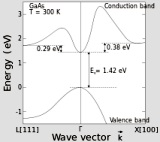

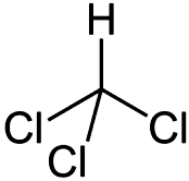 Methyl Chloroform
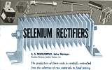 Selenium Rectifier
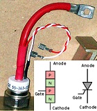 Thyristor
 Transistor Outline (TO) Package