Negative Feedback Transistor Amplifiers |
|||
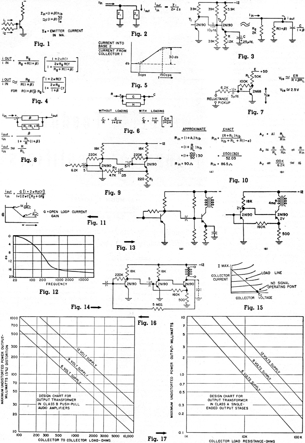
The big graphic with Figures 1 through 17 reminds me of the kinds of study sheets I used to make when cramming for exams in my college circuits courses. Did I ever tell you about the wise guy instructor I had for my first Circuits class at the University of Vermont? Anyway, this article provides an introductory level treatment of using negative feedback in amplifier circuits. Lots of illustration and formulas are included. Frequencies are at baseband, so you won't learn any secrets for high frequency amplifier stabilization, but then even RF and microwave circuits eventually need to convert down to baseband at some point for sampling or for use as audio or video. Negative Feedback Transistor Amplifiers By Hugh R. Lowry Manager, Application Engineering Semiconductor Products Dept. General Electric Co.
Complete design data for transistor negative feedback audio amplifiers with high-fidelity characteristics. Vacuum-tube audio amplifiers incorporating negative feedback have always been a popular item with the electronic hobbyist since there is a wealth of material in the literature giving design procedures and showing typical circuits which can be modified if desired. This situation is not true with transistor audio amplifiers because, until recently, most of the engineering effort has gone into developing circuits that will produce the maximum available gain from a transistor. This type of circuitry gives unsatisfactory results from transistor audio amplifiers since the frequency response tends to be limited, the distortion high, and the performance extremely dependent on the characteristics of the individual transistor. This article will describe how to design simple transistor negative feedback audio amplifiers that have characteristics good enough for even the "golden eared" group of audio enthusiasts. Before getting into actual circuits, however, it would be best first to review briefly a few basic facts about transistor circuits. The first important point about transistors is that their input impedance is quite low. As shown in Fig. 1, the input impedance is approximately Zin = (1 + β)•hib ≈ (1 + β)•(30/Ie), where β is the grounded-emitter current gain. Beta (β) is normally in the range of 30 to 100 making the input impedance roughly 1000 to 3000 ohms. With such a low input impedance, a transistor makes an excellent current adder. If two signals are fed from a source impedance high in comparison to the input impedance, the input current into the transistor will be essentially equal to the sum of these two currents. The second fundamental is the concept of a current divider as shown in Fig. 2. If a current source is fed into a network consisting of an impedance Z1 and Z2, the output current will be equivalent to Z1/(Z1 + Z2). An example of these two principles is the analysis of the low-frequency response of the circuit shown in Fig. 3. Here a transistor biased in the conventional manner is being fed from a transistor amplifier with a 3900 ohm load resistance. The equivalent circuit for low frequency may be approximated as shown on the right on Fig. 3. This equivalent circuit consists of a current source which is feeding into the parallel combination of a generator resistance and input impedance of the transistor. Since the input impedance of a transistor is equal to (1 + β) times the impedance of the emitter circuit, the emitter resistance must be multiplied by (1 + β) and the bypass capacitor will be divided by (1 + β). The formula for the transfer function is shown in Fig. 4 and it can be seen that if R(1 + β} is much larger than the generator resistance, the low-frequency 3 db point is determined only by the generator resistance, current gain, and the emitter bypass capacitor. In other words, the emitter bypass capacitor is not bypassing the emitter resistance, but is bypassing a resistance equal to the generator resistance divided by 1 + β. Fig. 5 shows the calculated frequency response of this circuit and it can be seen that even with a 25 μfd. bypass capacitor, the low-frequency response is down 3 db at 150 cycles.
These fundamentals will now be applied to the problem of high-fidelity audio amplifiers. To start off with, consider the case where a transistor is desired as a linear amplifier to work into a conventional vacuum-tube amplifier. It is also assumed that a variable reluctance pickup is to be used, that the supply voltage is 50 volts, and also that the emitter bypass capacitor be eliminated in order to obtain the best possible low-frequency response. A circuit that would meet these specifications is shown in the diagram Fig. 7. The biasing is done with a resistance from collector to base and with the circuit shown, the collector-to-emitter bias voltage will be about 2.5 volts. The items of interest would be the current gain, the voltage gain, and the input resistance. If the circuit is analyzed as a servo-amplifier, assuming that the feedback current and input current are added without interaction, the equivalent circuit is shown in Fig. 8. The feedback factor will be equal to the load resistance divided by the load resistance plus the feedback resistance. Putting this into the formula of a servo-amplifier with loading, the current gain is seen to be essentially the feedback resistance divided by the load resistance. At this point, the readers who are familiar with transistor circuitry are probably wondering how good these approximations are since, as is well known, a transistor is a bi-lateral device, there will be a forward transmission through the feedback loop as well as other considerations that must be included in an exact analysis. The degree of approximation can be seen from a comparison of the input resistance using the approximate and exact formulas as are shown in Fig. 10A. The approximate input resistance is equal to the current gain plus one times hib. Using this formula, the input resistance comes out 90 ohms. The exact expression for input resistance for this type of circuit is given in Shea's "Principles of Transistor Circuits" and is shown on the right hand side of Fig. 10A. A numerical evaluation of this formula gives the input impedance as 86.5 ohms as compared to 90 ohms from the approximate formula. In order to obtain the correct high-frequency roll-off with a reluctance cartridge, it should be loaded down with about 6200 ohms. Thus the circuit shown in Fig. 7 has 6,200 ohms in series with the signal and it is obvious that the difference between 86.5 and 90 ohms is of little significance in the design of this amplifier. The expression for voltage gain for this amplifier is shown in Fig. 10B and is approximately equal to the feedback resistance divided by the input resistance which in this case is about 16. One final point concerning this type of amplifier is that a radio-frequency type transistor such as the G-E 2N168 should be used because the output capacitance of a so-called p-n-p audio transistor is very high and if an audio transistor were used with a 50,000 load resistance, the high-frequency gain would begin to fall off at roughly 5000 to 10,000 cycles.
The simple amplifier, just described, is not suitable when followed by another transistor amplifier. If the next stage is a transistor, the input impedance of the following stage is very low and there would be essentially no a.c. feedback in the amplifier. There will, of course, be d.c. feedback to stabilize the operating point. A configuration suitable for transistor amplifiers is shown in Fig. 9. This circuit consists of two RC-coupled grounded emitter stages with negative current feedback from the emitter of the second transistor to the base of the first transistor. It is desirable to linearize the current gain with feedback since the input (reluctance pick-up plus 6,200 ohms series resistance) is essentially a current source. If the feedback capacitance is on the order of 5 μfd. the frequency response will be flat down to 20 cycles. By using a small capacitor, however, it is possible to effectively decrease the feedback at low frequencies and produce a bass boost. To compensate for the RIAA recording characteristics, the response of the preamplifier should have a 500-cycle turnover frequency with the response leveling out again near 50 cycles. Using the servo-amplifier analogy, an analysis of the configuration of Fig. 9 yields the expression of Fig. 11. The turnover frequency is determined by the time constant of the feedback circuit and the low-frequency response plateau is a function of the open loop current gain. The performance of an actual circuit is shown in Fig. 12 and it can be seen that it is comparable to conventional vacuum-tube circuits. By adding a resistor in shunt with the capacitor, a more positive control over the low-frequency plateau can be obtained. For example, for a 500-cycle turnover frequency the impedance of the capacitor at 500 cycles should be equal to R2. A 50-cycle low-frequency plateau is obtained if the resistor shunting C is made equal to 9R2. The biasing methods used in the amplifiers described thus far are suitable for RC-coupled amplifiers where the collector voltage is considerably smaller than the supply voltage. A problem arises, however, on the biasing of a driver stage which is transformer-coupled to the output stage. With a transformer load in the collector circuit, a biasing resistor from collector to base is no longer d.c. degenerative since the d.c. resistance in the collector circuit is small. One possible circuit for a small signal amplifier followed by a driver stage is shown in Fig. 13A. This type of biasing will stabilize the collector current of the driver stage, but a large bypass capacitor must be used for good low-frequency response as explained earlier. A better type of circuit is shown in Fig. 13B. The base of the driver stage is directly connected to the collector of the preceding stage and the emitter current of the driver stage is determined by the voltage at the base and the resistance in the emitter circuit. For the circuit shown, the bias current in the driver stage would be 4 ma. The biasing resistor to the base of the first stage is connected to the emitter of the driver stage rather than to the collector of the first transistor. This type of biasing by current feedback makes the bias points more stable than if each transistor were biased separately as in Fig. 13A. The reduction in the number of components by using direct coupling is also quite apparent. Perhaps the most important advantage of the direct-coupled circuit of Fig. 13B is that there are no capacitors to produce phase shift at low frequencies and possible instability. With this direct-coupled circuit it is possible to add another amplifier stage and use feedback around all three stages. A typical circuit of this type is shown in Fig. 14. The resistor from the collector of the driver stage to the base of the first stage makes the output voltage proportional to the input current which is very desirable. It is not necessary to use a d.c. blocking capacitor with the 5-megohm feedback resistance since the d.c. flowing through the resistor will not appreciably affect the bias point. If the driver transformer has a 5,000 ohm primary impedance, the overall current gain of the amplifier will be 5 megohms/5,000 ohms or 1,000 as calculated by the formula in Fig. 8. Depending on the frequency response of the transformer, it may be necessary to add a capacitor from the collector of the last transistor to ground in order to prevent high-frequency oscillations. High-frequency oscillations occur because the high-frequency phase shift produced by three cascaded stages is enough to make the feedback at high frequencies positive rather than negative unless precautions are taken. Class B Push-Pull Outputs
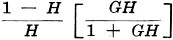
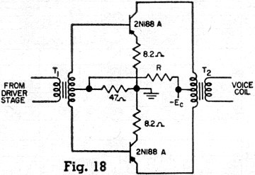
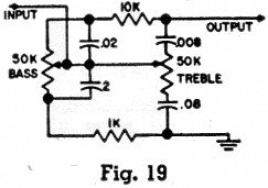
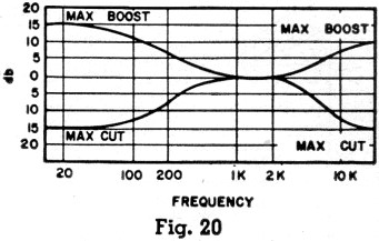
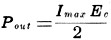
Fig. 21 & 22 - Two charts shown here indicate power gains that are obtained with commonly used transistors at various power outputs with a 12-volt supply. Chart at left is for class B push-pull amplifiers and chart at right is for class A single-ended circuits. Note higher output powers The design of driver and push-pull stages depends on the desired power output so it is necessary to start with the final stage and work backwards. In the majority of applications, the output power is specified so a design will usually begin at this point. The circuit of a typical push-pull class B output stage is shown by Fig. 18. The voltage divider, consisting of re-sistor R and the 47-ohm resistor, gives a slight forward bias on the transistors to prevent crossover distortion. Usually about 1/10 of a volt is sufficient to prevent crossover distortion and, under these conditions, the no-signal total collector current is about 3.0 ma. The 8.2 ohm resistors in the emitter leads stabilize the transistors so they will not go into thermal runaway when the junction temperature rises to 60° C. Typical collector characteristics with a load line are shown in Fig. 15. It can be shown that the maximum a.c. output power without clipping using a push-pull stage is given by the formula: Since the load resistance is equal to Thus, for a specified output power and supply voltage the collector-to-collector load resistance can be determined. For output power on the order of 50 mw. to 750 mw., the load impedance is so low that it is essentially a short circuit compared to the output impedance of the transistors. Thus, unlike small signal amplifiers, no attempt is made to match the output impedance of transistors in power output stages. The power gain is given by the formula: Since where: Rc-c = collector-to-collector load resistance Rb-b = base-to-base input resistance β = grounded-emitter current gain Since the load resistance is determined by the required maximum undistorted output power, the power gain can be written in terms of the maximum output power by combining equations (the previous equations) to give: Class A Driver Stages For a required output power of 250 mw., the typical gain for a push-pull output stage would be on the order of 23 db. Thus the input power to the output stage would be about 1 to 2 mw. The load resistance of a class A driver stage is then determined by the power that must be furnished to the output stage and this load resistance is given by the equation: For output powers on the order of a few milliwatts, the load resistance is not negligible in comparison to the output impedance of the transistors, therefore, more exact equations must be used to determine the power gain of a class A driver stage. From four- terminal network theory, after making appropriate approximations, it can be shown that the voltage gain is given by the formula: where: hib = grounded base input impedance. The current gain is given by the formula: where: hob = grounded base output admittance The power gain is the product of the current gain and the voltage gain, thus unlike the formula for high power output stages, there is no simple relationship between required output power and power gain for a class A driver amplifier. Design Charts Figs. 16, 17, 21, and 22 are design charts for determination of transformer impedances and typical power gains for class A driver stages and class B push-pull stages. Their use can be best understood by working through a typical example. It will be assumed that it is desired to design a driver and push-pull amplifier capable of delivering 1 watt with a 12-volt supply. Using Fig. 16, for 1 watt of undistorted output power, the required collector-to-collector load resistance is 200 ohms. From Fig. 21 using a typical 2N187A, the power gain is 20 db. In numerical terms, a power gain of 20 db is 100. Therefore, the required input power to the driver stage would be: Pin = 1000/100 or 10 mw. From Fig. 17, for 10 mw. of undistorted output power, the load resistance is over 5000 ohms. From Fig. 22, assuming a 2N191 driver transistor, the power gain is 38 db. The typical power gain of the two stages using a 2N191 driver and 2N187's in the output would be 58 db. The secondary impedance of the driving transformer should be 3000 ohms center-tapped. The secondary impedance of the output transformer should be selected to match the impedance of the load. A necessity for any hi-fi system is a set of tone controls to compensate for room acoustics, loudspeaker differences, listening level, and individual preferences. One acceptable circuit has been described in the literature1,2 and is shown in Fig. 19. The detailed operation is described in the reference but briefly at 1 kc. the incoming current divides so 10/11th is shunted to ground and 1/11th goes on to the next stage. The low- and high-frequency response depends on the potentiometer settings and can be analyzed on a current transfer basis. With the component values indicated, the performance of the tone controls is shown in Fig. 20. This performance is quite comparable to tone controls used with vacuum tubes. A circuit incorporating all design procedures herein described is shown in Fig. 23. This amplifier will produce more than enough undistorted output power for average listening levels in the home.
It can be seen that incorporating negative feedback in transistor amplifiers is quite simple with the main difference between transistor and tube circuits being that current feedback is used with transistors and voltage feedback with tubes. The use of current feedback in transistor amplifiers requires very few extra components and the performance advantages far outweigh the time taken in design.
References 1. Lo, Endres, Zawels, Waldhauer and Cheng: "Transistor Electronics," Prentice-Hall. 2. Lowry, Hugh R.: "All Transistor Hi-Fi Amplifier," Radio & Television News, November 1956.
Posted July 22, 2020 |
|||


 and the collector-to-collector
impedance is four times the load resistance per collector, the output power
is given by the formula:
and the collector-to-collector
impedance is four times the load resistance per collector, the output power
is given by the formula: 

 is equal to the current
gain, beta, for small load resistance, the power gain formula can be written
as:
is equal to the current
gain, beta, for small load resistance, the power gain formula can be written
as: