What's a MOS FET?
|
|
Usually when posting one of the Popular Electronics magazine quizzes that includes vacuum tubes, I suggest the reader mentally replace them with an enhancement mode FET. That is because like the tube, all configurations of FETs have a very high input impedance, which is why vacuum tube voltmeters (VTVMs) were used when it was important to not let the meter load down the circuit under test. Bipolar junction transistors (BJTs), by comparison, have relatively low input impedance, but are still useful as input buffers to mechanical meter movements. In 1967 when this article appeared in Radio-Electronics magazine, the MOSFET - or MOS FET as written at the time - was relatively new to the marketplace. A single 2N3608, made by the Microelectronics Division of Philco-Ford, cost $8.05 in 1967, which is equivalent to $72.65 as of this writing (per the BLS Inflation Calculator). Vacuum tubes were $1 to $2 apiece at the time. What's a MOS FET? - Newest type of transistor simplified
If the conventional junction-type transistor weren't already established, the MOS FET (Metal-Oxide Semiconductor Field-Effect Transistor) would have been developed instead. That's the opinion of many top scientists and engineers who have spent years experimenting with both kinds. Such comments suggest how dramatically versatile this new semiconductor is. The principle of the MOS FET† has been known for many years, but only recently has the state of the semiconductor art reached the point where practical MOS FET's could be manufactured on a production basis. Early MOS FET's were unstable and permanently affected by high temperatures.
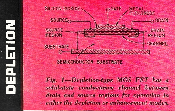
Fig. 1 - Depletion-type MOS FET has a solid-state conductance channel between drain and source regions for operation in either the depletion or enhancement modes.
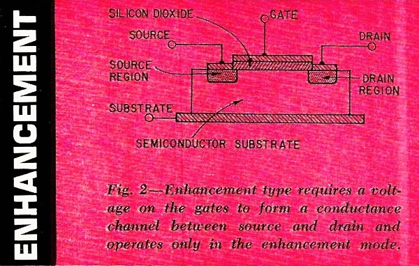
Fig. 2 - Enhancement type requires a voltage on the gates to form a conductance channel between source and drain and operates only in the enhancement mode. Some of the advantages of the MOS FET over other types of transistors: 1. A much higher input impedance 2. Lower noise 3. Lower stray capacitance 4. Better thermal stability 5. Wider frequency response 6. More uniformity from unit to unit. There are two types of MOS FET's: the depletion and the enhancement type. Fig. 1 is a simplified cross-section of the depletion type. Notice that the drain and source regions are connected by a very thin channel of n-type crystal. The gate lead is connected to a metal electrode which in turn is separated from the n-type semiconductor channel by a layer of silicon dioxide. This layer of silicon dioxide is extremely thin and is the secret to successful MOS FET operation. As is the case with the junction FET, appropriate bias voltages applied between gate and source electrodes can deplete the channel of its active current carriers. This is accomplished by the electric field in the gate region, very much like the action of a tube's grid. The conductivity of this MOS FET conduction channel can be "enhanced," or increased, as well as "depleted." Because the gate is well insulated and is nonrectifying (that is, no current can flow into or from the gate electrode) , the input resistance remains high with either type of operation and the power of the transistor is not affected. What's significant is that while current can flow through the MOS FET (from source to drain) with zero bias between the gate and the source, this current can be increased or decreased by applying the proper bias or signal voltage between these two electrodes. These two modes of operation, called the enhancement mode and depletion mode respectively, are both applicable to the depletion type. The current in the MOS FET does not cross a pn junction as in a conventional transistor. That eliminates minority-carrier problems and consequently many disadvantages inherent in the conventional transistor. Enhancement Type A simplified cross-section diagram of the enhancement type MOS FET is shown in Fig. 2. This type is identical to the depletion type except that the physical channel between the source and the drain does not exist. Because current cannot flow without some type of channel in a field-effect transistor, the enhancement-type MOS FET can be operated only in the enhancement mode. A bias must be applied between the gate and the source to "create" a channel. In Fig. 2, when a bias voltage is applied so that the gate is positive with respect to the source, electrons are drawn into the region beneath the gate electrode. With enough bias voltage, the p-type crystal immediately next to the gate and between the source and drain regions gains enough electrons so that it begins to act like an n-type crystal. Thus the necessary "channel" is formed. The width and conductivity of this channel are proportional to the voltage applied. Again the current can be controlled through the device without drawing any current from or into the gate electrode, leaving the input impedance very high at all times. While only n-channel devices have been mentioned so far, p-channel MOS FET's are also commercially available. The n- and the p-regions, and the polarities of the applied voltages, are reversed (as in pnp and npn transistors).
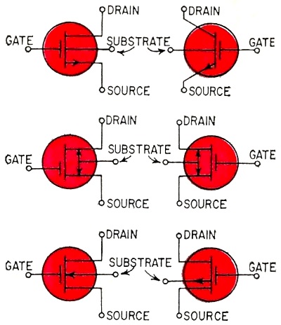
Fig. 3 - Unfortunately, MOS FET symbols appear to vary as the number of manufacturers. Here are just a few you will find in schematics. Unfortunately, symbols for MOS FET's are not yet standardized. Fig. 3 shows some of the symbols now used. All examples are n-channel type. The p-channel symbol is identical, except that the direction of the arrowheads is reversed. The substrate connection can be brought out of the case as a separate lead, or connected internally to the source electrode. Beware of Electrostatics The MOS FET isn't perfect - it has a disadvantage inherent to insulated-gate devices. It can easily become permanently damaged by a relatively low volt-age across its leads. The insulating layer of silicon dioxide to which the gate electrode is connected is made very thin to allow good control over the conducting channel with a low gate-to-source bias voltage. That same thinness allows this layer to be easily punctured. Because any current through this silicon dioxide layer results in permanent damage, a static charge on your body or clothes can ruin a MOS FET. A large electrostatic charge can accumulate on the electrodes if the MOS FET slides around in its packing material or if its leads are rubbed or brushed against clothing or other fabrics during handling. For this reason, MOS FET's (like meter movements) are usually shipped and stored with the leads tied together electrically with conductive foil or by some other means. Fig. 4 - Schematic diagram of the basic p-channel MOS FET preamplifier used to plot curves in Fig. 5. The PET can operate in a manner similar to a pentode vacuum tube. Fig. 5 - As the voltage across the drain and source increases, drain current increases. Operating point is the intersection of the load line and the line representing equal voltage across the gate and the drain, both with respect to the source. Load resistance RL is 12,000 ohms. Some precautions to prevent damage to MOS FET's (and all FET's) during handling and in circuits: 1. Always keep the leads connected together electrically until they are connected into a circuit. 2. Get the habit of watching for accumulation of potentially harmful static charges. Ground yourself and your equipment before handling FET's. 3. Use only soldering irons with grounded tips when working with MOS FET circuits. 4. Be sure the MOS FET and the circuit it is to be connected to are at the same potential before touching the two together. 5. Be sure that power supplies used with FET's do not produce excessive voltage transients, especially when they are turned on or off. These precautions shouldn't frighten you from taking advantage of these new devices. With proper handling, damage to MOS FET's should be extremely rare. After installation in the circuit, there is very little chance of damage because the circuit impedances should be low enough to prevent buildup of voltages high enough to cause damage. The MOS FET is especially good for preamplifiers, oscillators and other low-level circuits where high impedance and good frequency response are important. In many respects, it combines the advantages of both transistors and tubes, without their disadvantages. Resembles Pentode Tube A basic preamplifier circuit using an enhancement-type MOS FET is shown in Fig. 4. It can be used with a microphone, a phonograph or guitar pickup or for any other low-level signal application. The RF value isn't critical - it could be as high as several hundred megohms - because no gate current is drawn by the bias circuit. A nominal value would be 22 megs, which is large enough to present a high enough input impedance for most applications. If you want an extremely high input impedance, RF may be increased in value. The MOS FET shown in Fig. 4 is a 2N3608, made by the Microelectronics Division of Philco-Ford. Single-quantity price is $8.05. The resistance of RL is selected to match the characteristics of the MOS FET and other circuit values. Generally, as the resistance of RL is increased, voltage gain and output impedance in-crease, and input impedance decreases. The input impedance is approximately the RF value divided by the voltage gain. As an example of the process of selecting circuit values, refer to Fig. 5, a series of drain curves for the preamplifier. The dashed line represents the points where VGS equals VDS The load line is drawn for a supply of 18 volts with RL equal to 12k. The point of intersection of the load line and the dashed line represents the quiescent or self-bias point. Small-value coupling capacitors will work well with this preamp, because of the high impedances involved. Many possible applications for MOS FET's are only now coming into view. As cost drops, MOS FET's will show up more and more in commercial equipment. * General Dynamics Corp. † The MOS FET is sometimes referred to as an insulated-gate field-effect transistor (IG FET).
Posted June 28, 2023 |
|

 By Gene L. Jackson*