Transistor Circuitry: A Review of Transistor Characteristics and Operating Considerations |
|
Transistor basics have not changed since they were first introduced to the market around 1953. The first available transistors used germanium substrates, and then in 1954 Texas Instruments introduced the first commercial silicon transistor. The hybrid pi equivalent circuit for a PN junction transistor used in modern circuit simulators has many more 'virtual' components in it that allow for high frequency and nonlinear operation modeling, but for audio and AM type that operates entirely within the linear region, the equivalent circuit presented in Figure 1 will still get the job done. I remember in college in the mid 1980s running SPICE simulations on an IBM XT computer where the transistor model added a capacitor between the base and collector for simulating the Miller capacitance, and that was about it. Transistor Circuitry: A Review of Transistor Characteristics and Operating Considerations By Richard Clay,* W9JRO/4 Here is a general picture of transistor operation in simple terms. The two basic types of transistors are described and methods of using them in typical amplifier and oscillator circuits are outlined. If you've been thinking of experimenting with transistors this article will help you get off on the right track. Transistors have been available for quite some time and it is likely that certain amateurs will enjoy experimenting with them. Although they perform many of the functions of vacuum tubes, any effort to insert a transistor in a standard vacuum tube circuit will almost certainly be unsuccessful. In fact, the best general rule in designing a transistor circuit is to do exactly the opposite of what would be done in the similar vacuum tube circuit. It is the purpose of this article to outline the properties of transistors and show how to design circuits using them. It is quite unfortunate that there has been no standardization in the transistor industry. The names, characteristics, and prices vary between different producers. In order to avoid showing a preference toward any manufacturer the following circuits are given without reference to a particular transistor. In every case effort has been made to describe the considerations which lead to a proper choice for the circuit components. Construction of Transistors At the present time, transistors are made of the element germanium. When impurities are added to a crystal of germanium the electrical conductivity is changed in different directions through the crystal. Amateurs have been utilizing this effect for quite a few years with germanium diodes such as the 1N34. Antimony, arsenic, and phosphorus make what is called "n-type" germanium. The name arises from the fact that this type has an excess of free electrons, which are negative charges. Aluminum or boron make "p-type" germanium, which has a deficiency of electrons. Either type has greater conductivity in one direction than pure germanium, and the direction of best conductivity is opposite in the two types. There are two types of transistors. The so-c-alled "point-contact" type is made from a single crystal of n-type germanium. An electrode called the "base" is attached to one face of the crystal and two closely spaced contacts are made on the other face. These are called the "emitter" and "collector."
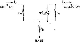
Fig. 1 - An equivalent circuit for a transistor. The current gain, α, corresponds to the amplification factor, p., in vacuum tubes.
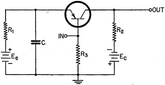
Fig. 2 - The grounded-base amplifier circuit. This circuit is stable with all types of transistors.
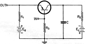
Fig. 3 - The grounded-emitter amplifier circuit. This circuit offers the greatest power gain and has characteristics which most closely resemble a vacuum tube amplifier.
Fig. 4 - The grounded-collector circuit. This circuit has properties similar to a cathode follower.
Fig. 5 - Resistance coupling in audio amplifiers. Because of the low emitter resistance of the second stage the condenser, C, must be much larger than normal for a vacuum tube amplifier.
Fig. 6 - Transformer coupling between stages. In order to match impedances a step-down transformer is used.
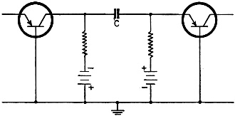
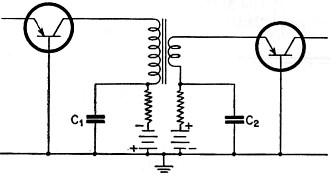
Fig. 7 - Series-resonant coupling for a tuned amplifier. At the resonant frequency of the L-C circuit maximum current is transferred to the emitter of the second stage.
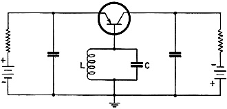
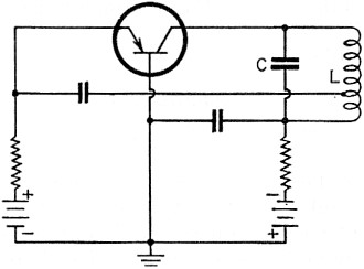
Fig. 8 - The parallel-resonant base oscillator circuit. This circuit will oscillate only when the current gain of the transistor is greater than one.
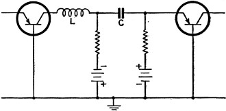
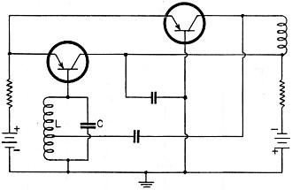
Fig. 9 - The grounded-emitter oscillator circuit. This circuit will oscillate with junction transistors.
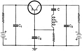
Fig. 10 - A transistor Hartley oscillator. Note that the emitter excitation has the same phase as the collector voltage.
Fig. 11 - An isolating oscillator using transistors. A grounded-collector stage (on the left) is used as the isolating amplifier. This circuit has not been tried at high frequencies. The "junction" transistor is formed of three layers of the two types of germanium. These may be arranged either as n-p-n or p-n-p. The n-p-n is the more common. In this type of transistor there are also three external connections. The base connection is made to the middle layer and the emitter and collector connections are made to the outer layers. The junction type has higher power dissipation, lower noise, and a cut-off frequency1 from 100 kc. to 1 Mc. The point-contact type has higher current gain and a cut-off frequency from 1 Mc. to 10 Mc. Certain types have been made to oscillate at frequencies up to 300 Mc. With either type the emitter is usually biased in the direction of high conductivity and this gives a low input impedance. The collector is biased in the direction of low conductivity and the output impedance is high. (Note that this is opposite to the situation with vacuum tubes.) Since the current flow is roughly the same for both the emitter and collector, the transistor offers considerable power gain, because of the high ratio of output to input impedance. Equivalent Circuit Fig. 1 shows an equivalent circuit for a transistor. The emitter resistance, Re, is a few hundred ohms. The collector resistance, Rc, is over 10,000 ohms for a point-contact transistor and usually over 1 megohm for junction transistors. It is important to note that the a.c. generator in the collector circuit is a current source. This is to be contrasted with the usual vacuum tube equivalent circuit which uses a voltage source. The factor α is the current gain and corresponds to the voltage gain or amplification factor, μ, in vacuum tubes. There is no phase reversal in transistors. An increase in emitter voltage and current causes increases of the same polarity in the collector circuit. This fact is tremendously important in designing transistor circuits. Amplifier Circuits Fig. 2 shows one type of amplifier circuit, called the "grounded base" circuit. This is a stable circuit with both types of transistors and gives a power gain from 20 to 40 db. The input and output impedances are approximately the same as the emitter and collector resistances of the transistor so this circuit has a low input impedance and a high output impedance. The indicated polarities of Ee and Ec are proper for both n-p-n and point-contact transistors. If a p-n-p transistor is used, the polarities should be reversed. Either an examination of the characteristic curves or the manufacturer's specifications will show the proper emitter and collector currents. The resistors, R1 and R2, are chosen to give the proper currents through the emitter and collector. Usually Ee and Ec are low-voltage sources such as a 22.5-volt battery. With this type of source R1 and R2 will be around 10,000 to 20,000 ohms. The internal resistance from the emitter to the base is not constant in most transistors. This means that the input circuit presents a load to the source which varies during portions of the cycle. In order to minimize distortion it is frequently necessary to insert a resistance, R3, in series with the emitter circuit. The value of this resistance is best found by experiment. Fig. 3 shows the "grounded emitter" circuit. This circuit may be unstable with point-contact transistors because the current gain in this type is greater than one. Since there is no phase reversal in transistors, base potential fluctuations due to the collector current provide a regenerative effect and may lead to oscillation when a point-contact transistor is used. This circuit will then become a relaxation oscillator and will generate nonsinusoidal waves. This circuit has a higher input impedance and a lower output impedance than the grounded base circuit. It has the highest power gain of any of the simple amplifier circuits and most closely resembles a standard vacuum tube amplifier. Resistors R1 and R2 are again chosen to give the proper operating currents to the emitter and collector. However, the flow of collector current through R3 provides a self-biasing effect for the emitter circuit similar to a cathode resistor in a vacuum tube circuit, so R1 will have a higher value in this circuit than in the grounded base circuit. The base resistor, R3, is usually around 10,000 ohms. The condenser, C, by-passes the emitter to ground. For certain values of R3 the self-biasing effect is adequate and the emitter, may be grounded directly. The "grounded collector" circuit is shown in Fig. 4. This circuit resembles a cathode follower in vacuum tube circuits and is likely to be unstable when a point-contact transistor is used. It has the highest input impedance, the lowest output impedance, and the lowest power gain of all the basic circuits. The voltage gain is slightly less than one. The circuit considerations are similar to those for the grounded emitter circuit except that the by-pass condenser, C, is placed from collector to ground. Interstage Coupling The peculiar properties of transistors must be considered when designing interstage coupling. It must be remembered that transistors are essentially current-actuated devices and have very low input impedances. For applications requiring compact construction it is possible to use resistance coupling in audio amplifiers as shown in Fig. 5. Grounded-base amplifiers are shown but this method applies equally well to grounded-emitter stages. The voltages and resistances are selected as described previously. Because of the low emitter resistance in the second stage the condenser, C, must be very large. It is commonly around 0.25 μf., and may be as large as 10 μf. if good low-frequency response is desired. Transformer coupling can also be used and the basic circuit is shown in Fig. 6. This type of circuit can be used for any frequency at which the transistor will provide gain. In r.f. and i.f. amplifiers the primary is tuned. The voltages and resistances are chosen to provide the proper bias currents to the collector and emitter. The capacitors, C1 and C2, are by-pass condensers and maintain the a.c. voltage drop across the transformer windings. In an audio amplifier the transformer has a primary designed around 10,000 to 20,000 ohms and a secondary for 100 to 500 ohms. A standard plate-to-line transformer can frequently be used. It is important to note that any interstage transformer will be of the step-down type because this type steps up the current and thus provides greater drive for the next stage. This again is quite opposed to common practice in vacuum tube circuits. In tuned amplifiers a very useful type of coupling is that shown in Fig. 7. This may appear very strange until it is realized that a series L-C circuit acts like a short circuit at the resonant frequency. At this frequency the maximum current will be transferred from the collector of the first stage to the emitter of the second stage. The gain will be greatest at the series-resonant frequency. The emitter resistance of the second stage is in series with the resonant circuit so for sharpest tuning this resistance should be as low as possible. Oscillators The type of oscillator circuit to be used depends a great deal on the type of transistor used. Perhaps the most common oscillator circuit used with point-contact transistors is the parallel-resonant base circuit shown in Fig. 8. With the point-contact type α is greater than 1 so the collector current which flows through the tank circuit can be greater than the original emitter current. Since this collector current flows in a negative direction the combined effect is that of a negative resistance across the tank circuit. This is the requirement for sustained oscillation. It is interesting to note that no tapped coils are necessary. This is essentially due to the fact that the transistor has no phase reversal. The capacitors from emitter and collector to ground are by-pass condensers and are chosen so as to be appropriate for the frequency at which the circuit oscillates. A rather common oscillator circuit for junction transistors is the grounded-emitter circuit shown in Fig. 9. It derives its name from the fact that C1 is so large as to provide the emitter with an effective a.c. ground. When this circuit is analyzed it is found that a negative resistance appears across the series-tuned tank circuit. Condensers C2 and C3 form a voltage divider. Part of the collector current flows through C2 and provides the emitter voltage necessary to sustain oscillation. For frequencies in the intermediate range C2 and C3 are around 0.01 μf. The Hartley oscillator circuit for transistors is shown in Fig. 10. This circuit has oscillated readily for the author. Since there is no phase reversal in transistors it is necessary to excite the emitter with a voltage which is in phase with the collector voltage. Therefore, in this circuit both emitter and collector are connected to the same side of a.c. ground in the tank circuit. This should be contrasted with the vacuum tube Hartley oscillator circuit where the grid and plate are connected to opposite sides of the a.c. ground. In the March, 1953, issue of QST the author described a vacuum-tube oscillator circuit in which an isolating amplifier was used to remove the loading effects of the oscillator tube from the tank circuit. Since transistors have inherently low resistances they provide a rather heavy load on a tank circuit and it seemed wise to try the same trick with transistors. The transistor analog of a cathode follower is the grounded collector circuit so this circuit was used as the isolating stage. The remainder of the circuit shown in Fig. 11 was conceived from basic considerations. The transistor on the left is the grounded-collector isolating stage. It was a pleasant surprise to find that the circuit oscillated the first time it was turned on. Since junction transistors were used, the oscillation could not have been due to the grounded collector stage alone. Because of the low cut-off frequency of the transistors used it was not possible to maintain oscillation past the usual intermediate frequencies. Therefore, no information could be obtained regarding the stability of this circuit when used at the higher frequencies for which the original isolating oscillator was designed. In conclusion, it should be emphasized that although transistors have received wide publicity which in some cases has suggested that they are a panacea for all the ills of electronics, for the present at least they have rather restricted application, especially in the amateur field. The amateur and experimenter will do well to realize this fact and to regard them as rather expensive toys. He should most certainly forego the pleasures of playing with them until he feels well grounded in the basic considerations which lead to sound transistor circuitry. * RCA Engineer. 1 The cut-off frequency is defined as the frequency at which the gain is down 3 db. as compared with the gain at low frequencies. In general, the cut-off point for voltage gain is different from that for current gain.
Posted January 11, 2016 |
|