Practical Applications of Simple Math - Part III
|
|||||
Many people were (and still are) reluctant to approach the theoretical aspect of electronics as it applied to circuit design and analysis. QST (the ARRL's monthly publication) often included equations and explanations in many of their project building articles. Occasionally, an article was published that dealt specifically with how to use simple mathematics. This "Practical Applications of Simple Math" piece in the July 1944 edition of QST is the third installation of at least a four-part tutorial covering resistance and reactance, amplifier biasing, oscillators, feedback circuits, etc. I do not have Part I from the May 1944 edition or Part IV from the August 1944 edition, but if you want to send me those editions, I'll be glad to scan and post them (see Part II here). Practical Applications of Simple Math: Part III - Resistance-Coupled Amplifier Calculations By Edward M. Noll* EX-W3FQJ
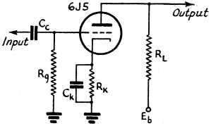
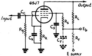
The design of a resistance-coupled amplifier is a relatively simple operation involving considerably less formula juggling and mental exertion than computing all the deductions subtracted from your pay check these days. The information given in previous installments of this series, plus some added information on the practical use of vacuum-tube characteristic curves, will permit the ready calculation of all required design values for the resistance-coupled amplifier shown in Fig. 1. The characteristic curves for the type 6J5 tube are shown in Fig. 2. The Ep/Ip curves, the most common in general use, show the variations in plate current with changes in plate voltage for various fixed values of grid bias, the complete set of curves forming a "family" of characteristics for the particular tube under consideration. These curves represent static variations in tube potentials and currents when the tube circuit is not loaded. When a load is applied, such as the plate resistor of a resistance-coupled amplifier, an additional line called the load line must be drawn to represent the dynamic variations in tube potentials and currents. It is apparent that the .plate-current variations through the load resistance cause a varying voltage drop across the plate resistance, which is actually a change in plate voltage. Thus, a change in grid potential with the applied signal does not change the plate current without changing the plate voltage. In fact, the resultant change in plate voltage, caused by the variations of plate current through the load resistance, represents the useful output of the amplifier. Therefore, a load line representing the plate load resistance (total resistance between plate and cathode) is drawn on the characteristic curves to show the actual dynamic changes in tube operation. Many excellent articles have been written on the theory of characteristic curves and load lines. Since this article is aimed at illustrating the practical application of the curves, theoretical considerations will be brought into the discussion only when necessary. Constructing the Load Line In constructing the load line on the characteristic curves, the actual resistance of the load depends upon the circumstances under which the amplifier is to be operated. Each set of conditions may require a slightly different value of load resistance for optimum performance. Optimum values may be chosen, for instance, for maximum possible undistorted voltage output with a given value of input signal, or for maximum possible undistorted voltage output with a definite amount of plate supply voltage. Each of these requirements may necessitate the use of different values. As an illustration of the method used in arriving at the first of these objectives, let us assume that the maximum peak-to-peak signal delivered to the grid of the amplifier of Fig. 1 from the preceding stage is 8 volts. It is necessary to place the load line on the curves in such a position as to permit the signal to swing over the linear portion of the characteristic curves. Therefore the signal must not swing into the curved portions at low plate-current values, nor must it swing into the positive grid distortion region. In the case of the 6J5 triode curves the least value of bias that can be employed with an 8-volt signal is -4 volts, permitting the signal to swing between 0 and -8 volts. Bias in excess of -4 volts should not be used because it would result in an undesirable reduction in gain. As a result, the load line must be drawn to permit the grid signal to swing over the linear region, between the 0- and -8-volt bias curves. The actual load line might be drawn at any one of a number of different slopes and in each case the plate voltage swing each side of the mean value would be equal and therefore distortionless. However, we are interested in obtaining a maximum plate-voltage swing with a low value of average plate current and a minimum variation in plate current. From this consideration, it is evident that the load line should appear practically horizontal and well down on the characteristic curves. Since a load line which approaches a horizontal position represents a high value of resistance (large change in plate voltage with a small change in plate current) the resistance-coupled voltage amplifier has a high value of plate resistance in comparison to a power amplifier, where we are interested in a large plate-current variation to develop power. Thus we find our 6J5 load line for an 8-volt signal well down on the curve; in fact, point B on the-8-volt curve was chosen as far down as possible without moving into the region of distortion as indicated by excessive curvature. Using the point on the -8-volt curve as one point of the load line, a straightedge is moved about this point as a pivot until an equal plate voltage is set off by the swing of the signal on each side of the average bias value set on the -4-volt curve. When this position is found, a line is drawn along the straightedge which represents the value of plate resistance which permits maximum nondistorted voltage output. The value of this resistance is readily calculated by extending the load line until it crosses the plate-voltage and plate-current coordinates, as shown in Fig. 2. The slope of the load line, or the resistance represented by the load line, is equal to the change in plate voltage divided by the change in plate current. Maximum Voltage Gain We are now ready to consider Some typical problems. 1) What should the total plate load resistance, Rp, be for maximum undistorted voltage gain in the amplifier of Fig. 1, using the characteristics shown in Fig. 2? From Fig. 2 we find that the slope of the load line is
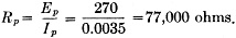
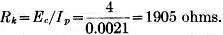
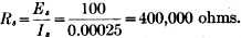
2) Find the plate power-supply voltage, Eb, required. Since the maximum plate voltage is applied to the plate only when no plate current flows through the load, the plate voltage indicated at zero plate current is the power-supply voltage. The position at which the load line crosses the zero plate-current axis is point C, representing 270 volts. Therefore, Eb=270 volts. 3) Calculate the required value of the cathode resistor, Rk. Examination of the curve shows that the average plate current at our operating bias, point O, is equal to 2.1 ma. Therefore, the resistance required to develop this amount of bias across the cathode resistor is
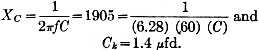
4) Calculate the required value of the plate load resistor, RL. Since the total plate resistance includes the cathode-biasing resistance, the actual value required for the plate resistor is the total plate resistance minus the value of the cathode resistor, or RL = Rp - Rk = 77,000 - 1900 = 75,100 ohms. 5) Determine the value of the grid resistor, Rg. The value of the grid resistor should be at least four times greater than the plate load resistor of the previous stage, but should not exceed the maximum value set by the tube manufacturer for safe operation of the tube. In the case of the 6J5, the maximum value set by the manufacturers when using cathode bias is 1 megohm. In most cases the value used is in the vicinity of 500,000 ohms. 6) Determine the value of the cathode bypass condenser, Ck. The capacity of the cathode bypass condenser is set at a value which will pass the lowest frequency to be amplified with a gain equal to 70.7 percent of the gain over the middle range of frequencies. (The calculation of capacity values will be elaborated upon in the next installment. However, it is a basic rule that, if the reactance of the condenser at the lowest frequency is equal to the resistor value, the amplifier response will be down 70.7 per cent at this frequency.) Since Rk is equal to 1900 ohms, the reactance of Ck for a minimum frequency of 60 cycles should be 1905 ohms. The minimum capacity for Ck may then be determined as follows:
7) Determine the value of the coupling condenser, Cc. The coupling condenser, which also causes a loss of low frequencies because of its reactance, is calculated in like manner with respect to the grid resistor, or
8) Determine the. peak plate-voltage and plate-current variations. By dropping perpendicular lines to the coordinates from the points A, O, and B in Fig. 2, which represent the average bias and the extremities of grid-signal swing, the peak-to-peak plate voltage and current can be determined by simple subtraction. Peak-to-peak plate voltage = 175 - 40 = 135 Peak-to-peak plate current = 3 - 1.25 = 1.75 ma.
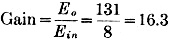
9) Determine the peak-to-peak voltage output of the tube. Since the plate-voltage swing represents the variations in potential between plate and cathode, the portion of the variation across the cathode resistor is lost. The actual voltage output, Eo, of the stage is
Eo = 131 volts
10) Determine the voltage gain of the amplifier stage. Voltage gain is equal to the output voltage divided by the input voltage.
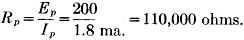
Maximum Power Output Let us consider now the case where it is desired to obtain maximum possible undistorted output for a selected plate-supply voltage. As an example, in the circuit of Fig. 3 a supply voltage of 200 (Eb) is assumed. Since the maximum value of 200 volts is applied to the 6SJ7 plate only when no plate current flows, one point on our load line is certain to be at point A, shown in Fig. 4, where the plate current is zero and the plate voltage 200. From point A, load lines of various slopes may originate; the lower the plate load resistance, the steeper the slope. Since, as in the previous example, we are only interested in obtaining a large plate-voltage variation with a minimum variation in plate current, the slope of our load line should be as far down on the curves as possible and still accommodate the complete grid swing without running into the distortion region. Therefore, two typical load lines were drawn on the curves shown in Fig. 4. The load line AB represents a load resistance of 13,000 ohms which provides for a 5-volt grid signal without distortion, while load line AC represents a load of 110,000 ohms which provides for a 1-volt signal. Load-line AC would be the most common, since the 65J7 is a high-gain pentode which is designed to amplify small input signals to a much higher level.
Inspection of the curve shows that we are operating the tube at a negative bias of 4 1/2 volts and that the negative peak of the grid signal reaches -4 volts. In the case of a triode, such an amplifier would not be operating under optimum conditions. However, the presence of the screen and suppressor in the pentode permits the plate voltage and plate current to swing to very low values without distorting even on the higher-bias curves. Thus we can obtain a large plate-voltage variation at reasonable efficiency if we do not permit the signal to approach zero on its positive peak. From the information available we may now proceed to calculate suitable circuit values and some of the operating conditions:
1) Find the total plate resistance represented by the load line, AC.
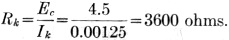
2) Find the proper value for the cathode resistor Rk. Since the bias point, midway between points D and E which represent the extremities of permissible grid swing without distortion, is at -4 1/2 volts, the average plate-current flow is 1 ma. and our average plate voltage is 80 volts. The screen current is approximately 25 percent of the average plate current and, therefore, the total current passing through Rk is 1.25 ma. In order to secure a 4 1/2 volt drop, the value of Rk is
3) What should be the value of the plate resistor, RL? RL = Rp - Rk = 110,000 - 3600 = 106,400 ohms.
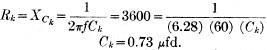
4) Determine the value of the cathode condenser, Ck.
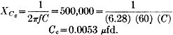
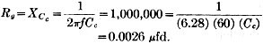
5) What should be the value of the coupling condenser, Cc, when using a 1-meqohm grid resistor, Rg?
6) The value of the screen-dropping resistor, Rs, is readily calculated if the screen voltage and screen current are known. The screen potential must be 100 volts to meet the requirements of the characteristic curves, which are drawn for a screen potential of 100 volts. Therefore, the voltage drop required across the series screen resistor is 200 - 100 = 100 volts.
7) In order to bypass the screen-dropping resistor adequately, the reactance of the bypass condenser, Ck, should be not more than 1/10th the resistance of the screen-resistor at the lowest frequency.
8) If the resistance-coupled amplifier is employed in an audio system which has three or more stages, it may be necessary to employ a decoupling network, RfCf to prevent feedback through the common plate impedance. In this case, the power supply voltage must be increased by an amount sufficient to compensate for the voltage drop across Rf. The value of Rf often employed is 1/10 of the value of RL. Rf = (0.1) (106,400) = 10,600 ohms.
9) The condenser Cf bypassing Rf, should have a reactance, at the lowest frequency to be passed, of not more than 10 percent of the resistance of Rf.
10) The new supply voltage would, of necessity, be 200 volts plus the voltage drop across RF. E = 200 + (Is + Ip) Rf = 200 + (0.00025 + 0.001) (10,600)
11) The total plate-voltage swing as determined by the perpendiculars
of Fig. 4 is 130-30 = 150 volts. From the ratio,
If a different screen voltage were selected the curves would change somewhat, calling for alterations in the values. In the next installment, covering the design of a two-stage audio amplifier, an approximate method will be outlined to convert the curves to a lower screen potential.
Posted September 7, 2023 |
|||||


 , we
know that 97 percent of the output voltage or 97 volts peak-to-peak appears across
the plate resistor. Since a 1-volt peak-to-peak signal is applied at the grid, the
stage gain is 97/1 = 97.
, we
know that 97 percent of the output voltage or 97 volts peak-to-peak appears across
the plate resistor. Since a 1-volt peak-to-peak signal is applied at the grid, the
stage gain is 97/1 = 97.