Solid State - Charged Coupled Device
|
|
From the mid 1950s and through mid 1970s, Popular Electronics magazine ran a series of articles entitled "Solid State" in order to facilitate the electronics industry's effort to move people from vacuum tubes to semiconductors. In fact, if Solid State ran every months since its beginning, this being installment 182 means it began in 1956 - just eight years after the transistor was invented. Even though the commercial industry had already shifted to almost exclusively transistorized products, a large part of the consumer base had been raised on tube radios and televisions. In this case, the news is in regard to Bell Telephone Labs' recent invention of the semiconductor charge coupled device (CCD) - the heart of all modern imaging systems. Prior to the CCD, a vidicon tube, which as the name suggests was a glass-encapsulated vacuum component, did the job, only with much less resolution, much greater volume occupied, much higher current and voltage requirements, and at a much higher cost. Solid State columns: April 1967, August 1967, April 1966, August 1970, July 1971, October 1971, April 1972. Solid State
Scientists and engineers at Bell Telephone Laboratories (Mountain Avenue, Murray Hill, NJ 07974) have developed a new solid-state device which, one day, may provide an exciting new field for the serious experimenter and hobbyist. Using charge-coupling techniques, the device scans printed matter, drawings or photographs line-by-line, converting variations in light intensity into electrical signals. If transmitted to remote locations over telephone lines or by radio broadcast, these signals can be used to reproduce high resolution images of the original material. The new imaging device is a 2-mm by 4.5-mm chip of homogenous p-type silicon semiconductor with an insulating layer of silicon dioxide overlaying the silicon and a linear array of 288 separate metal electrodes deposited on the oxide surface a mere 12.5 microns apart. These 288 electrodes are connected electrically into three groups: one consists of the 1st, 4th, 7th, etc., electrodes; another the 2nd, 5th, 8th, etc.; and the last the 3rd, 6th, 9th, etc., electrodes. The first three electrodes operate as a single light-sensitive element, as do each subsequent group of three, for a total of 96 elements.
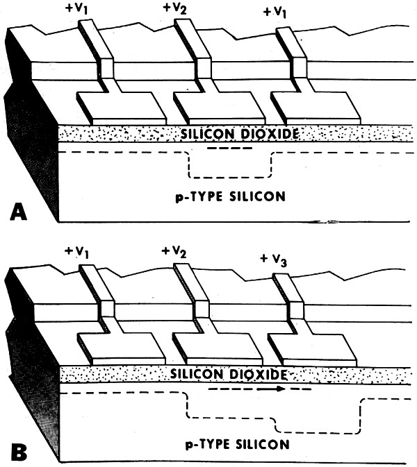
Fig. 1 - How signal charges are kept and moved on in Bell Lab's charge-coupled imaging device. Charge storage is shown at A, while B shows how charge transfers when an adjacent electrode is raised to a higher positive potential. It would appear that an all solid-state TV camera using the device may not be too far off. In operation, a lens is used to focus an image on the surface of the silicon chip. Light from the document or other material releases negatively charged minority carriers (electrons) within the silicon, with more charges generated where the light is brighter, fewer where the light is dimmer. Within each sensing element, the center electrode is connected to a more positive voltage with respect to the silicon substrate than the other two, as illustrated in Fig. 1A. Charges generated by the light near that element collect at the surface of the silicon under the center electrode. Since the number of collected charges at each element is proportional to the light flux falling on the silicon at that point during the accumulation (storage) period, the resulting concentration of charges is a linear measure of the light and dark areas on the original material. In the experimental device assembled at Bell Labs, the charge pattern is accumulated in only 2.5 milliseconds. At the end of the accumulation period, the groups of stored charges are transferred along the surface of the silicon by successively applying a more positive voltage to the electrode adjacent to the one holding the charge, while decreasing the voltage on the electrode over the charge region, as shown in Fig. 1B. This causes the charge to move from under one electrode to under the next electrode. Called charge coupling, this transfer process is repeated sequentially until each charge packet has passed along the array of electrodes to the end of the device. When they reach the last electrode, the charges are collected by an output electrode connected to a small n-type diffusion in the p-type substrate at the end of the structure. A positive voltage is applied to this electrode, reverse biasing the p-n junction and developing an electrical field within the silicon which attracts the charges to the n-type region, thus generating an electrical current whose fluctuations represent variations in light intensity along a line of the original image. Signal read-out from the device requires only about 96 microseconds. Since the imaging device handles but a single line along one dimension, the document being scanned must be moved relative to the device either optically or physically to develop a two-dimensional image signal. In the initial experimental system, then, the basic set-up included a light source to illuminate the document, a lens to focus its image on the sensor's surface, a drive mechanism to move the document from line to line as it is scanned, the silicon image sensor, and, of course, the necessary electronic circuitry to develop charge packet transfer and read-out. Despite the experimental nature of the initial system, the images are of exceptional quality. Bell expects even better resolution and definition as the imaging sensor's design is refined and fabrication techniques are improved. Still in its developmental stage, Bell's new solid-state image sensor probably will not be available as a commercial device for many months. When offered on the general market, however, it should be useful in a variety of interesting projects, ranging from low-cost facsimile systems to reading aids for the blind, from industrial comparison instruments to image decoders, and from slow-scan television to electronic locks. One day, perhaps, the new device might even find an application in an automatic fingerprint analyzer, thus joining other electronic devices in the never-ending war on crime.
Posted June 24, 2019 |
|