Solid State - Early Mention of GaAs
|
|
When is the last time you heard someone refer to electronics as "solid state?" It was a necessary differentiator during the era of transition from vacuum tubes to semiconductors. Mere utterance caused fear in some, and futuristic hope in others. "Solid State" was a big buzz phrase in marketing to household consumers and industry planners. Why, I ask, was "solid state" chosen as the term to counter vacuum tube electronics? Did we ever refer to tubes as "gaseous state" or "plasma state" devices? Maybe the "solid" part of "solid state" evoked a sympathetic emotion with the coincident hippie / beatnik era population's usage of the adjective "solid," meaning "right-on," "I agree," "I understand," or maybe "cool!" Yes, I know the technical definition of solid state and that it is an apt description of semiconductors, but it seems to me a more effective term could have been coined, like Miniature Amorphous Germanium Intrinsic Component (MAGIC) or some other acronym based on focus group polling. Oh yeah, focus groups hadn't been invented yet in the 1960's. My primary reason for presenting this article is the mention of gallium arsenide (GaAs) as a semiconductor. Also, "gc." in this article means gigacycles per second (GHz). Update: An RF Cafe visitor wrote to say he and his colleagues in the 60's and 70's jokingly referred to vacuum tubes a GasFET's, GlassFET's, and GlowFET's. Solid State columns: April 1967, August 1967, April 1966, August 1970, July 1971, October 1971, April 1972. Solid State - GaAs Mentioned By Lou Garner, Semiconductor Editor
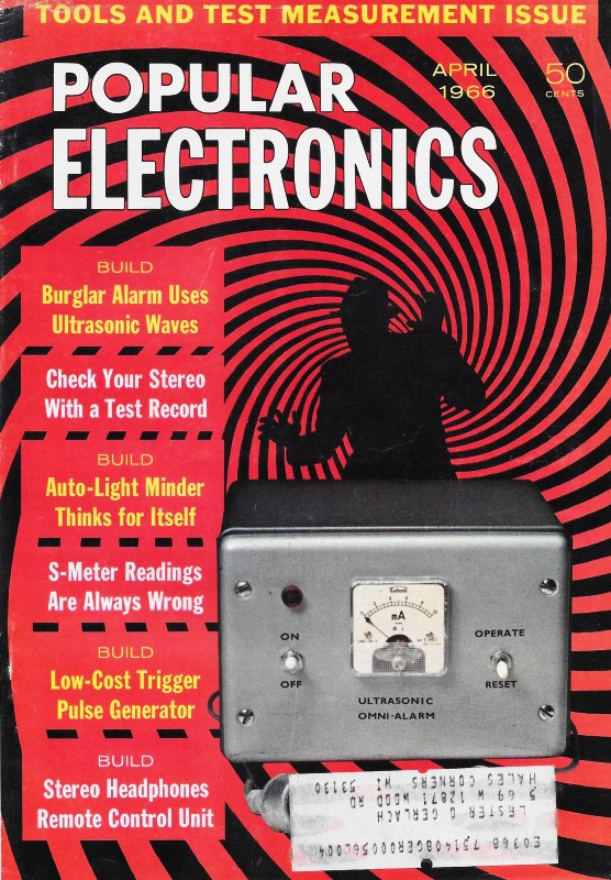
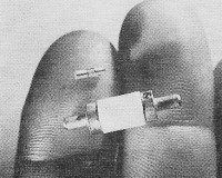
The relative size of two transit time devices being investigated at Bell Labs for use as microwave generators and amplifiers is shown above. The smaller device contains a tiny wafer of gallium arsenide. The larger device is used to house either a Read diode or a silicon pn junction diode. Unless you're an advanced experimenter, student, or ham, new developments in the microwave field may seem far removed from your day-to-day interests. Yet, the advanced technique of today can become rather commonplace within a relatively short time. The transistor itself is but one example. When first developed, the transistor was an expensive, difficult-to-use laboratory curiosity. In less than five years after its introduction, however, medium-priced units became available for hobbyist applications and, today, the transistor is perhaps the most popular of all experimenter components. In our opinion, something similar will occur with the new generation of semiconductor devices now being investigated by Bell Telephone Laboratories (New York, N.Y.). These devices, which may one day replace medium-power special-purpose vacuum tubes in microwave applications, have already generated as much as 60 milliwatts of continuous r.f. power in the 2-11 gigacycle range (2,000 to 11,000 megacycles). Three types of devices are now under study at Bell Labs: a bulk gallium arsenide device, a silicon avalanche diode, and a Read avalanche diode. All three have been operated as self-excited oscillators, generating microwave frequencies when driven by a d.c. voltage. In addition, they have been used as amplifiers in conjunction with external stabilizing circuitry. A common characteristic of these devices is that their operating frequency is determined, in part, by the transit time of the electrons through a region in the semiconductor material. The transit time is generally comparable to one cycle of the device's operating frequency. In contrast, the time required by electric charges traveling through the junctions of other solid state devices, e.g., conventional transistors and tunnel diodes, corresponds to only a small fraction of a cycle. Thus, it is possible to design the new structures in such a way that the volume of the material actively used in generating microwave energy is greater than that of conventional devices operating at the same frequency. This allows the new devices to operate at relatively higher voltages and power levels. Appropriately, they are called "transit time" devices. The bulk gallium arsenide device consists simply of a piece of n-type gallium arsenide to which two metal contacts have been affixed. (See Fig. 1.) At Bell Labs, continuous microwaves have been generated in bulk gallium arsenide in the frequency range of 2-3 (gc.), with outputs exceeding 60 milliwatts and efficiencies of between 5% and 6%. Furthermore, amplification of signals in the 2-10 gc. range was achieved with gains of 4-5 db at bandwidths of 600-700 mc.
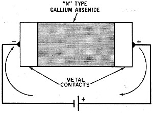
Fig. 1. Bulk gallium arsenide device is made by sandwiching n-type gallium arsenide between two metal contacts. The arrows show the current flow. Both the silicon and the Read transit time devices are made from semiconductors containing a junction which is reverse-biased to produce avalanche breakdown. (Avalanche is a high field discharge caused by internal secondary emission which is not destructive to the junction.) The avalanche region is either inside or adjoins the high field transit region. The Read avalanche diode was first proposed by W. T. Read of Bell Labs in 1957. Made of silicon, this diode has a complex internal electrical structure consisting of alternate p, n, i, and n semiconductor layers, thus forming a pnip device. Using a Read diode, scientists have generated continuous oscillations at 5.2 gc. with an output of 19 milliwatts and an efficiency of 1.5%. Don't rush to your corner distributor to buy test units. These transit time devices are still in their experimental stages. But you might check with your distributor in two or three years. Manufacturer's Circuit. Since we talked about field-effect transistors (FET's) in this column, a number of readers have requested that we show some circuits. In anticipation of the day when low-cost FET's will be available in quantity for experimental purposes, here's a hi-fi tone control (Fig. 2) you can experiment with. One of several related circuits suggested by Siliconix, Inc. (1140 W. Evelyn Ave., Sunnyvale, Calif. 94086), the tone control features a single FET as a high-impedance buffer amplifier, with frequency response controlled by RC tuned feedback loops. Gate bias for Q1 is established by source resistor R8, bypassed by C5, while R7 serves as the drain load. Capacitors C1 and C6 are, respectively, the input d.c. blocking capacitor and output coupling capacitor. In operation, part of the input signal is applied through isolation resistor R1 to the bass tone control network, C2, R2, and C3. The bass response is determined by R2's setting in conjunction with the feedback signal coupled from Q1's output through R6, and which appears across R5. Resistors R6 and R5 form a voltage-divider network. Similarly, the rest of the input signal is applied across the circuit's treble control, R4. Treble response is determined by R4's setting, the value of C$, and by the output signal fed back to R4. Except for R2, the 1-megohm potentiometer used as a bass control, and R4, the center-tapped 500,000-ohm potentiometer used as a treble control, all resistors are half-watters. Capacitors C1, C2, C3, C4 and C6 are small ceramic types, while C5 is a 25-volt electrolytic. Transistor Q1 is a 2N2843 FET. Operating power is supplied by a 22-volt battery or a conventional line-operated d.c. power supply.
Fig. 2. Hi-fi FET tone control by Siliconix, Inc., uses a twin-T notch filter to obtain 40-50 db attenuation at the notch frequency when output load impedance is near infinity. Circuit can also be used in a negative feedback loop of another FET amplifier to produce narrow bandpass characteristics.
Fig. 3. By placing diodes in the coil circuits to block a reverse polarity current, and by systematically reversing the polarity of the control current, a 2-wire line can be used to separately control each of three relays. In addition, if proper values are selected for the circuit components, a low-frequency current can control all relays at once. Furthermore, if individual RC values are carefully selected, each relay can be made to respond to its particular frequency while rejecting all other frequencies. The circuit can be wired on a conventional chassis, on a perforated phenolic board, or on a special etched-circuit board, as preferred. The completed tone control can be used as a separate circuit for experimental purposes or, depending on individual needs, as part of a more complex audio preamplifier design. Transitips. With low-cost transistors, SCR's and similar devices in plentiful supply, many hobbyists are likely to forget that the common diode is an extremely versatile and useful device. The diode's ability to rectify a.c. and to block d.c. of reverse polarity can be utilized in a number of control circuits. One such circuit is shown in Fig. 3. Here, a 2-wire control line is used to operate anyone of three relays at will. The relays, K1 , K2, and K3, are similar types. All of the diodes, too, are similar, and can be general-purpose units. Networks R1-C1 and R2-C2 are of the simple a.c. filter type, and C3 serves as a d.c. blocking capacitor. Actual values must be determined by circuit requirements, types of relays used, and mode of operation. Let's see how the circuit works. Suppose we wanted to close relay K1. We would simply apply a d.c. voltage of the indicated polarity to the control line. Under these conditions, D1 is biased in its forward direction, permitting a current flow through K1's coil, and thus actuating the relay. At the same time, D2, being reverse-biased, blocks any current flow through K2's coil. Relay K3 would not operate either, because of the presence of C3 with its d.c. blocking action. To actuate K2, we need simply to reverse control line polarity. Relay K2 would then close, while K1 and K3 would remain open. To actuate K3, we would apply a low-frequency a.c. signal to the control line. Filter networks R1-C1 and R2-C2 would act to prevent the application of adequate signal to energize their respective relays. On the other hand, the a.c. signal passing through C3 would be rectified by bridge rectifier D3 through D6 and applied to K3's coil, actuating this relay. Thus, the a.c. would activate K3 without affecting the state of K1 or K2. With a proper choice of component values, we could also actuate all three relays simultaneously, by applying a low-frequency a.c. signal to the control line. Under these conditions, filters R1-C1 and R2-C2 would become less effective, permitting the control signal to be rectified by diodes D1 and D2, and thus actuating their respective relays. Relay K3 would continue to operate as with a higher frequency signal. With a variety of control signals to choose from, component values could be selected to permit the following modes of operation: (1) Relay K1 contacts closed with d.c. of a given polarity, other relays open. (2) Relay K2 contacts closed with d.c. of reverse polarity, other relays open. (3) Relay K3 contacts closed with high-frequency a.c., other relays open. (4) Relays K1 , K2, and K3 closed with medium-frequency a.c. (5) Relays K1 and K2 closed with low-frequency a.c., relay K3 open. And it's all done with the aid of diodes! Unless I'm reading my calendar wrong, Spring is about ready to bust out all over ... have you planned any "sunny day" projects?
Posted April 13, 2018 |
|