Receiver Noise from Antenna to Detector
|
|
Here from a 1965 issue of Electronics World magazine is a really nice write-up on electrical noise, both how it originates and how it affects receiver systems. Although vacuum tubes were still the predominant active amplification components in 1965 (the date of this article), semiconductors were already solidly ensconced in the signal detector role. I have to confess to learning a new term that I probably should be familiar with: Equivalent-Noise-Sideband-Input, or ENSI. It appears also in Reference Data for Engineers: Radio, Electronics, Computer, and Communications. Interestingly, this is the first time in a long time I have seen noise referred to as "grass;" the drawings make it clear why the moniker was created. We were taught to use "grass" in USAF radar tech school and used it in common parlance once on duty as radar technicians. Receiver Noise from Antenna to Detector
The sensitivity of a radio receiver is governed by the amount of internally generated noise, how this noise originates, how it is measured, and how it can be reduced are covered in this article. The most common byproduct of our civilized world is noise in one form or another. We rise in the morning to noise; we ride to and from work with noise; and we eat and relax with noise. In its most common form, noise is the effect of vibration upon our eardrums, and subsequently through the message centers of our nervous system, upon our brain. In electronics, however, noise is a different matter. More than being just annoying, it is the limiting factor in the reception of intelligence through the medium we call communications. The ultimate goal is the reception of intelligence and the reproduction of the originally transmitted material in its truest fidelity, whether the receiver be a simple table radio or an extremely complicated and sensitive piece of electronic laboratory equipment. The weak signal received at the antenna must be amplified, sorted out of the myriad of other signals and assorted electrical impulses, amplified to a greater degree than the undesired signals and noises, converted to a varying d.c. voltage by a detector, and then applied to functional circuits to actuate a speaker, CRT, relay, or any of a multitude of recording devices. Kinds of Noise
Fig. 1. - (A) Passband of receiver showing both desired and interfering signal. (B) Detector output with and without a.g.c. Bias change due to a.g.c. can reduce or eliminate desired signal when the interfering signal is present
Fig. 2. - If the interfering signals shown on the right occur between T1 and T2, their relatively short duration and low amplitude have no effect. If situation is reversed, receiver would then be blocked for that period of time. The various types of noise can be broken down into two basic categories: natural and man-made. There are various methods of dealing with noise, but no matter what the source, there is a limit to the amount of reduction we can achieve. Man-made noise includes both intentional and unintentional signals within the passband of the receiver; interference from sparking, such as automotive ignition, arcing of generator or electric motor brushes, and defective wiring; and a host of other causes, most of which result from an electric spark. Such a spark produces interference over an extremely wide frequency range and is impossible to filter out if it is near the level of the signal to be received. Intentional signals might include those that are produced within the passband of the receiver, either due to drift of the transmitter or poor design of the receiver. Such a signal, if strong enough in intensity, will cause the first few stages of the receiver to draw grid current and hence block (in the case of tubes) or saturate (in the case of transistors). If automatic gain control (a.v.c. or a.g.c.) is used, the strong undesired signal will cause drastic reduction in the gain of the stage or stages, and the desired signal will then be amplified to such a small degree that it will be unintelligible or unusable. (Fig. 1.) This effect is known as cross-modulation, and its effects are determined by the type of tube used in the r.f. or i.f. stages, the bandpass of the receiver, the shape factor of the selective circuits (relation of peak to skirt bandwidth), and the type of interference. If the interference has a different time relation or duration than the desired signal, it may have little or no effect on the intelligibility of the received signal. (Fig. 2.) Another effect of undesirable signals within the passband is known as intermodulation distortion. Intermodulation distortion results when an interfering signal is applied to the mixer along with the desired signal. The non-linearity of the mixer produces both sums and differences of the two, in addition to the modulation of one by the amplitude variations (modulation) of the other. In addition to this, if the interfering signal produces cross-modulation sufficient to bias the r.f. stage back to a non-linear point, then the r.f. stage itself will act like a mixer and produce its own sums and differences, which will then be passed on to the mixer stage to further produce sums and differences of those that get through the passband of the r.f.-output, mixer-input circuits. Natural interference causes noise in a form we call static. Such interference results from lightning, aurora, whistlers, and, to some extent, so-called galactic noise. Lightning, or other static electricity, produces a spark during discharge, and hence yields the same result as man-made static. The only difference here is that the intensity of a lightning discharge is tremendous and in most cases completely blanks out the receiver, whether or not the signals coming through are desired or undesired. Aurora, on the other hand, produces a wide variety of effects, from sizzling static to rapid fade or flutter, not to mention the complete blanketing of electromagnetic circuits such as telephone lines. Whistlers are usually of short duration and, because of Doppler effect, change frequency to some degree as they progress. Depending upon the selectivity of the receiver, they may pass completely out of the passband before the a.g.c. can react. Galactic noises, except for u.h.f. and microwave receivers, and some v.l.f. equipment, with antennas designed specifically for the reception of these fixed noises, are not of any significance to the average reception medium, since the inverse-square law of r.f. signal strength vs distance shows them to be too minute. It is the natural law that makes the intentional reception of these stages difficult in radio astronomy. Galactic noises are so weak that other noises tend to obscure them, and the search for better reception methods is an unending one. Receiver noise, other than that due to antenna or cable defects, is the most important factor to consider. Since the antenna itself is essentially a passive device, there is no significant noise contribution from it other than that received by it in the form of the electrical radio signals. In most cases, the sensitivity of a receiver is set solely by the front-end of that receiver itself; that is, between the antenna terminals and the first i.f, stage. Because the r.f. stage, mixer, or first i.f. stage can contribute to this sensitivity, they must be considered separately and together. Defining Sensitivity
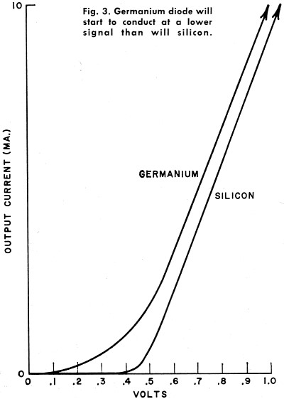
Fig. 3. - Germanium diode will start to conduct at a lower signal than will silicon. The relation among sensitivity, gain, detector levels, and selectivity seems to be a confusing one to many, yet each is a separate entity. Further confusion is often added by the concept of noise, signal-to-noise ratio, noise figure, and noise voltage. It is one aim of this article to clarify the meanings and relationship among these terms. Sensitivity means just what it says. It is the degree to which a receiver is sensitive to a signal. In other words, a more sensitive receiver will be able to reproduce the same intelligence from a smaller amplitude signal, all other things being equal. A less sensitive receiver will require a larger signal, all other conditions being the same. However, the sensitivity at the input end will also depend upon the amount of gain, or amplification, that follows it and the level desired or obtained at the detector. By a detector, we mean the point at which r.f. is converted to d.c., AM, or any other type of intelligence. For practical purposes in this discussion, let us consider the receiver as being a high-frequency communications or radar receiver with a diode detector, the intelligence being in the form of positive square pulses. This is something that could be observed on an oscilloscope and thus serves well to aid in the explanation. Because of the characteristics of the usual r.f.-type silicon or germanium diode detector, the last i.f. stage must have sufficient output to drive the detector well into the linear region. For most of these diodes, the output must be at least 0.5 volt to produce a minimum of distortion and good linearity of the modulation. (Fig. 3.) If we put a pulsed signal into the receiver and increase its level until we can see a small output from the detector but no random noise, we have no way of knowing the actual sensitivity of the receiver. Additional amplification between the r.f. stage and the detector might show either of two things: the increase of output signal level resulting might also be accompanied by the appearance of noise such that any decrease in input signal would cause the output signal to disappear into the noise; and a decrease in input signal would still produce an output with no visible noise. If additional gain produces noise at the output, no further gain would help and, for the given conditions, the maximum sensitivity of the receiver has been attained. This is also known as the threshold sensitivity. If, however, no noise appears, the receiver still has inadequate gain between the r.f. stage and the detector, and the sensitivity can be further improved by additional stages of gain. This should be increased to the point where noise does begin to appear in the output, and we are then at the same point discussed previously. The point of adequate amplification has been reached when sufficient noise is seen at the detector output. This noise level should be about 0.5 volt or half the desired 1.0-volt signal. Front-End The selectivity of the front-end is the ability of the receiver to receive or reject certain signals close to each other, Thus selectivity means to select, to reduce or remove interference, and reduce cross-modulation and intermodulation interference. Traps and bandpass transformers eliminate specific signals that are sufficiently displaced from the desired signals and limit those that are not sufficiently out of the passband to be rejected completely. The greatest amount of receiver noise is due to the action of electrons within the first tube or transistor. If the first stage is a converter rather than an r.f. stage, then the relative noise out of the receiver will be greater for a given input signal level. If a mixer (converter) stage follows an r.f. stage but the r.f. stage has little gain, then the relative noise level out of the receiver may be somewhere between the two levels. This will be explained subsequently. Origin of Noise Even in the most perfect component, some noise is always developed due to the random motion of free electrons within the material. Since the velocity of the electrons represents current flow, then a varying a.c.-voltage component is produced due to the natural resistance of the material. Because electron motion is always random, so is its velocity, and hence the frequency and amplitude of the noise voltages are continuously changing. The net result is called white noise, and its energy is evenly distributed throughout the entire radio spectrum. Because the r.m.s. voltage taken over a relatively long period of time is measurable, we know that for a given bandwidth the voltage would be the same at 100 kc. as. it would at 100 mc. because of this even distribution. This noise voltage, when due to the antenna and transmission line, is usually negligible compared to the tube or transistor noise and is further dependent upon the temperature, the resistance across which the noise voltage is developed, and the bandwidth of the component, circuit, or receiver. Although the average noise voltage is zero, the a.c. component exists in cycles varying in a perfectly random manner and has a constant r.m.s. voltage. The mean-square noise voltage associated with the input circuit is found by: en2 = 4kTRă, showing that the noise is dependent upon the temperature (T), bandwidth (ă), and the equivalent input resistance (or noise resistance) for the first stage (R) k is a natural constant, a relation of energy-per-degree of temperature discovered by Boltzmann. In a vacuum tube, random emission and random velocities of the electrons as they leave the cathode or arrive at the plate produce a random modulation of the d.c. plate current component known as "shot noise," If a tube is relatively noisy, then the equivalent resistance in the grid circuit is quite high. Hence, the merit of a tube in relation to its noise contribution is dependent upon how low an equivalent resistance can be assumed to be present in the grid circuit. This equivalent resistance for a triode is simply 2.5/Gm, but for a pentode it is much higher because the electron stream is divided into two paths - plate and screen - and the random modulation of the d.c. plate component is considerably greater. For any given tube type, there is a value of source resistance for which the best noise figure of that tube can be achieved. This information has been calculated for various types and is normally found in the manufacturer's data sheet for that tube. For transistors, the information is usually given as a typical noise figure at some test frequency, with a fixed-source impedance. In addition, curves are often shown that give the range of frequencies over which the transistor or tube is usable, and these show both the variation in noise figure with frequency and the difference in noise figure with different source impedances. Except for the filaments, a transistor presents a similar problem in relation to noise. Since the flow of electrons (or holes) in both cases is from a lower to a higher energy level, the same sort of thermal agitation takes place, and the modulation of collector current produces a noise voltage. The transistor, however, because of its base-spreading resistance, methods of biasing, and impedances, has until recently resulted in a relatively high noise level. For the sake of discussion, however, the terms tube and transistor may be used interchangeably.
Fig. 4. - Typical input circuits. (Top) Vacuum-tube cascode. (Bottom) Grounded (common) emitter circuit. Except for the bias and input circuits, r.f. circuit is similar in both. As the frequency is increased, there are further effects of transit-time loading with a reduction in gain that appears to increase the noise of the stage, and the equivalent input resistance seems to be as much as five times greater. If the signal and the noise in the first stage are amplified sufficiently, then all the noise added by the next stage will be hardly significant. For example, if the noise voltage at the input of the first stage is one microvolt, and the signal is two microvolts (representing a 2:1, or a 6 db signal/noise ratio), and the gain of the stage is 20 (or 26 dbv ), then the noise . voltage and signal voltage at the input of the next stage will be 20 and 40 microvolts respectively. If the next stage then adds one microvolt of noise to this, then it represents an increase of 1/20 or 5%. The third stage, if the second stage is similar to the first, will then add 1/400 or 0.25%. The formula for this is usually given as: NFtotal = NF1 + (NF2/Gain1) where NF represents the noise figure of that stage in db. It is therefore essential that the first stage have the lowest possible noise contribution with the highest possible gain. Because the lowest noise figure in a tube is obtained with a triode, this is normally used as the input stage, or more often, two triodes in a cascade circuit are employed (Fig. 4). This circuit comprises a low-noise triode in a grounded-cathode stage with little or no gain, to eliminate Miller effect (change in tube capacitance with gain change from a.g.c.), followed by a grounded-grid stage with the gain of a pentode, to eliminate the grid-plate capacitance feedback problem. The cathode impedance of the second stage, usually a few hundred ohms, serves as a low-impedance output load for the first stage, thus making this section extremely stable. Transistors, until recently, were notorious for their noise and could not be used as input stages where good sensitivity was desired. As a result, hybrid receivers were constructed, with input stages using low-noise vacuum-tube circuits (usually the cascode) followed by transistor circuits for the mixer and i.f, amplifiers. Recent improvements in semiconductor materials have resulted in germanium transistors with noise figures of 2 db up to several hundred megacycles and silicon transistors with noise figures near 3 db for the same frequency ranges. The nearest devices until then were the low-noise triode tubes, such as the W-E 417B, and the more recent RCA nuvistors and G-E ceramic subminiature triodes, but these required considerably more power for the active elements. Noisy Converters
Fig. 5. - Detector outputs. Top row, left to right: output, no visible noise; increased gain, still no noise; same condition, noise visible, shows adequate gain; signal reduced to original 1-volt level, noise disappears, signal good; noise level approaching that of signal. Bottom row, left to right: adequate gain and noise figure; gain not improved but noise reduced; same as last case but with additional gain after first stage, over-all signal still good; last condition shows maximum sensitivity (tangential sensitivity) when bottom of noise in pulse is equal to top of noise outside. At reasonably low frequencies (up to 500 mc.), there is a definite advantage to the use of one or more r.f. stages to give adequate amplification with minimum noise contribution. Because the conversion gain of a triode used as a mixer (again the less noisy tube) is less than its gain as an amplifier, noise contribution can be minimized if the gain of the preceding stage or stages is adequate. The input equivalent resistance as a mixer is 4/Gm, instead of the 2.5/Gm as an amplifier, and the conversion noise figure is higher than that of the amplifier noise figure. At some high frequency, known as the transition frequency, the use of an r.f. amplifier ahead of the mixer becomes impractical because of the transit-time loading effect, excessive feedback, insufficient gain, and other problems. In this case, the signals are fed directly to a converter or mixer. This may consist of a special tube circuit or, at the higher frequencies where the reactances within the tubes or transistors cannot be tuned out, the use of mixer crystals or diodes is preferred. These are usually preceded by tuned circuits or cavities to provide the necessary selectivity to eliminate images or other interfering signals within the passband of the following circuits. Because there is no amplification in this type of converter, and even a loss in signal during the conversion process, the first i.f. stage then becomes an important factor in the over-all noise of the receiver. In this case, the total noise figure becomes: NFtotal + L (NFi.f. + t - 1) where L is the diode conversion loss and t is the diode noise temperature. The total noise then obviously rests heavily upon the noise contribution of the i.f. amplifier. Just as in the case of the r.f. stages, the first i.f. stage must have highest gain and lowest noise in order to have a minimum noise contribution from the i.f. stages as a whole when this system is operating. Matching Considerations Of equal importance in the consideration of low-noise circuitry is the matching of impedances between antenna and input stage, or input stage and mixer. Aside from the consideration of maximum power transfer, it is essential to provide the match from the source to the correct input noise impedance. It is only under these conditions that the minimum noise conditions can be achieved. In transistor circuits, some designers intentionally load down the input circuits with excessive damping resistance in order to make the stage more stable. This is often done at the sacrifice of gain, since this additional power is dissipated uselessly in the loading resistor. If such excessive loading is attempted, it should not only provide the correct noise-match impedance, but it should also be done by using the low input impedance of the transistor itself. In this way the excess power is not dissipated in a resistor but instead is dissipated as useful power within the active elements of the transistor, providing a stable amplifier but with more gain (and hence better sensitivity for the same noise voltage). This is the ideal solution. Measuring Noise
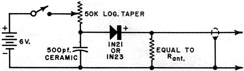
Fig. 6. - A simple noise generator. The output is fed to receiver antenna terminals while the input circuits are adjusted for maximum noise for fixed settings of noise potentiometer. We have discussed the requirements of receivers with respect to noise, and in order to obtain the best possible noise figure for a receiver, it is necessary to make some adjustments. A noise generator as an outside noise source is quite often used in laboratories, but a calibrated signal generator may also be used. A noise generator uses a temperature-limited diode, also known as a noise diode, with a variable anode current source. Because the noise output has a wide spectrum and its amplitude is directly related to the anode current, the generator can be calibrated directly in noise figure. It is connected through suitable d.c. isolation to the receiver input. The input is shunted by a resistive termination equal to the antenna impedance, and the noise power at the receiver output is measured. The anode current of the noise generator is then increased until the noise power out of the receiver has been doubled. The noise figure (usually in decibels) is then read directly off the generator. Theoretically, this represents the number of db of noise greater than a perfect receiver where all of the noise was due to the antenna. This perfect receiver would then have a noise figure of zero db. The indicator for output power may be an oscilloscope, a peak-reading v.t.v.m., or a thermocouple indicator. When reading voltage, the power is doubled when the voltage is increased by 1.414 times the original value. The noise factor is then F = 20IbRant, where Ib is the anode current of the noise diode and Rant is the equivalent antenna, or receiver input impedance. When trying to optimize the performance of a given receiver for best noise figure, it is not necessary to have an actual noise figure. A noise generator may be made from a high-frequency diode, and the receiver circuit is then adjusted for minimum relative noise. Such a generator is shown in Fig. 6. The signal-generator method depends largely upon the bandwidth of the receiver and the linearity of the detector. If the detector level is adequate, as discussed earlier, the measurement may be considered quite reliable. The standard of receiver measurement is that of the equivalent-noise-sideband-input,
or ensi. In this method, the unmodulated carrier is applied to the input of the
receiver (always through its proper antenna impedance) and the noise power is read
on an r.m.s.-reading instrument. This level should be three to ten times as great
as the expected noise voltage, or about 2 to 5 volts. The carrier, still at the
same level, should now be modulated at 400 cps and 30%. The signal-power output
is then measured through a filter that will pass only 400 cycles (this eliminates
the problem of different bandwidths in the receivers). The ensi is then equal to
Initially, it is necessary to select a tube or transistor with a good noise figure. This information, along with the best noise-match impedance, is usually provided in the manufacturer's data sheet. Sometimes it is necessary to use some other impedance, or because of supply voltages available, it is not possible to duplicate the manufacturer's test conditions exactly. In this case, the best conditions must be arrived at. A triode tube usually produces the best noise figure when it is biased for class A operation where the gain is maximized, consistent with linearity. In a transistor, it is most often found that the best noise figure is obtained when the collector current is quite small, usually around 1 to 2 ma. Depending upon the circuitry, it is usually advantageous to adjust the matching transformer and its loading for best noise figure. By observing a signal (either on an oscilloscope, or modulation through a 400-cycle filter) , adjust for the greatest signal-to-noise ratio for a given generator output. When the noise match has been optimized, the smallest input signal will be seen above the noise. The noise figure may be further improved in a grounded-cathode tube circuit, or in a common-emitter transistor circuit, by neutralization. This reduces the effects of the grid-plate or base-collector capacitance upon the input impedance. The usual practice is to place a small inductance between the grid and plate through a series-blocking capacitor. When the reactance of the inductor is equivalent to the reactance of the grid-plate capacitor, the two will be in parallel resonance, and the effect is the same as replacing the capacitive reactance with a very high series reactance of the value of QX, the "Q" of the inductance, and the reactance of either the coil or capacitor. It will be found that the maximum noise voltage, maximum gain, and maximum sensitivity will result simultaneously with the best noise figure. Do not look at the noise voltage alone when adjusting for best noise figure, as this is deceiving. A signal must be visible with the noise in order to determine whether or not the ratio of signal to noise has increased or decreased with an increase in noise voltage. See Fig. 5.
Posted March 30, 2020(original 6/4/2015) |
|
 By Joseph Tartas


 where Es is
the unmodulated carrier level, and Pn and Ps are unmodulated
and modulated output power, respectively.
where Es is
the unmodulated carrier level, and Pn and Ps are unmodulated
and modulated output power, respectively.