Flexible Printed Wiring
|
|
This is the last of a series of articles on printed circuit boards (PCBs) that appeared in the October 1969 issue of Electronics World, reporting on the latest and greatest advances in printed circuit board technology. Author Gaetano Viglione, of Sanders Associates (bought by Lockheed Martin in the 1980s and now owned by BEA Systems), reported on the state of the art of flexible printed circuit wiring. Sanders did a lot of aerospace and military electronics systems and was a leader in the field. In those days, the larger electronics manufacturers had their own in-house PCB design and fabrication capability. Flexible Printed Wiring By Gaetano T. Viglione / Manager, Product R & D Flexiprint Division, Sanders Associates, Inc.
The author is a graduate of Columbia University (Chemical Engineering). He holds several patents in metal processing and chemical engineering. He has been a consultant to industry and federal government in process engineering problems. This wiring can be preformed, folded and rolled, twisted and turned to fit any conceivable irregular configuration. It is particularly useful in very dense electronic packages. Flexible printed circuitry consists of flat etched copper conductors bonded between layers of pliable insulation. While this sounds simple enough, flexible printed circuitry has had placed upon it many demands, some of which are due to the numerous design features which appear to be attainable. The use of flexible circuitry as an interconnection medium has begun to inspire the design engineer because of its many advantages. For example, the significant difference of less weight per unit of area coupled with the reduction of volume over conventional cabling techniques, results in reductions in mass of 2:1 and, in some cases, 8:1. The feature of flexibility allows circuits to be preformed, folded and rolled, or twisted and turned to fit any conceivable irregular configuration in the more dense electronic packages, especially those typical of aerospace applications. Further, flexible printed circuitry is readily shielded and inherently more reliable due to its design and the adaptation and use of materials having exceptional physical properties.
Table 1 - Characteristics of the most commonly used insulation material for flexible printed wiring. The real dollar savings come at the time of assembly of the electronic package because of a reduction in man-hours required for assembly. Another benefit is the reduced possibility of error when connecting by flexible printed circuitry as compared to the greater possibility of error when using point-to-point wiring. Listing of Advantages The benefits resulting from the use of flexible printed wiring and cabling include the following: 1. Each circuit is a finished unit, ready for component assembly. 2. Handling of individual wires is eliminated because there is no need to measure, cut, strip, tin, route, solder, and lace. 3. Circuits are custom-designed for each job; therefore, wiring errors are eliminated. 4. Each circuit of a particular design is mechanically and electrically identical and completely repeatable. 5. Solder pads are in one place, rendering them ideal for automatic processing. 6. Wiring requirements no longer limit package geometry. Circuits can be run flat, bent around sharp corners, folded, and twisted. 7. Conductor breakage is nil. High-reliability hinge, spring return, and extensible interconnections can be readily designed. 8. Flexible printed circuitry can be bonded to rigid circuit boards to create a complete, one-piece interconnection assembly, eliminating unnecessary solder joints. 9. Single and multilayer circuits are closely spaced and held to close tolerances; therefore, high wiring and internal package densities are possible. 10. Flexible printed circuitry has a high volumetric efficiency. Close-tolerance conductor location is possible because each circuit is a precision etched unit. 11. Material normally needed in the form of a relief loop for the bend radius using standard wire cable can be eliminated, resulting in shorter wiring runs. 12. Thin, flat, two-dimensional geometry permits cable routing through narrow slots and along smooth surfaces, eliminating the excessive bulk of round wire. 13. Depending on the specific application, flexible printed circuitry can save approximately 75% of volume and weight over conventional round-wire cable.
Fig. 1 - Conductor widths and spacings for various thicknesses. 14. Foreign material, such as moisture, flux, and gases which could "wick" inside the insulation of wire, cannot degrade flexible printed-circuit performance because all conductors are completely encapsulated. 15. Tension loads are carried by the entire cable, not by individual wires; therefore, each circuit part is a solid mechanical structure. 16. High reliability in demanding environments is inherent because the entire circuit flexes as a unit under stress of vibration and shock. 17. Distributed capacitance and cross coupling do not vary from unit to unit of a single design, resulting in constant electrical characteristics. 18. Circuits are easier to solder and inspect than a tangle of conventional wires; therefore, quality-control operations are more accurate. Design Criteria & Costs When considering the use of flexible circuitry for interconnecting either printed-circuit boards or black boxes, certain basic design criteria should be remembered. General guidelines to keep the number of layers in flexible circuitry to a minimum are: set-up pin address to reduce or eliminate crossovers; use the freedom of pin address as a method of reducing layers; consider the use of narrower conductors and spacing; and use fold-outs to increase density at the terminal area. There are many factors that affect the cost of a flexible circuit. Major cost advantages result if standard flexible-circuit materials and sizes are used and if non-critical tolerances are loose enough to allow economical, automated production. The following items will also serve to keep costs to a minimum: 1. Specify 0.0027" thick (2-ounce) copper conductors if possible. These are the most economical because raw materials are purchased, handled, and stocked in large quantities. Other sizes, such as 0.00135" (1 ounce) and 0.0040" (3 ounces) are available should the need arise. 2. Specify enlarged punched-out areas in the covercoat at solder-pad areas rather than tight-fitting, pad-sized individually punched areas. This eases registration in manufacturing and thereby reduces cost. 3. Try to keep punched-out bare copper areas on the same side of the circuit. If it is necessary to present bare copper on the reverse side of a circuit, try to eliminate the extra cost involved in punching the base insulation by folding the circuit. 4. Keep large punched-out areas in simple shapes to lower the cost of intricate dies and/or to avoid excessive hand-cutting and punching. 5. Design terminal pads somewhat oversized to allow for slight drift. 6. Specify insulation as shown in Table 1. These are usually stocked in quantity. 7. It is recommended that conductor widths be specified larger than the minimum shown in Fig. 1. 8. It is recommended that conductor spacing be specified larger than the minimum shown in Fig. 1. 9 . Hold over-all flexible-circuit length and width to a minimum. 10. Use the fewest number of layers possible.
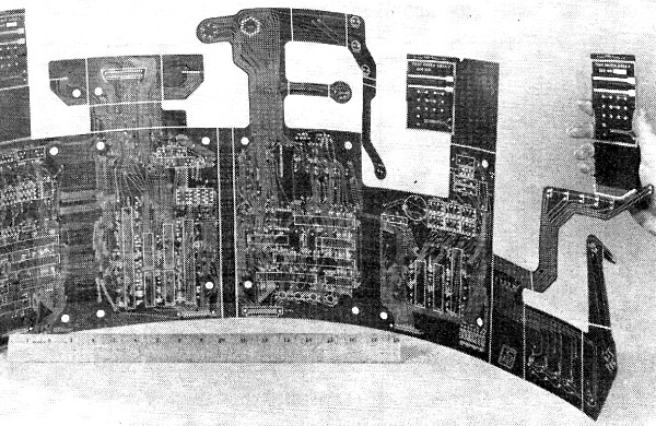
This complex flexible printed circuit, which is shown here along with an 18-in rule for size comparison, demonstrates how a complicated interconnection problem has been handled.
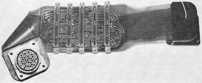
A multilayer flexible circuit with layer-to-layer interconnections along with connectors attached is illustrated. Terminating Methods Another important design consideration is the selection of the termination method. Recently, connectors for flat cable that accommodate circuits of 50-mil centers have become available. The type and size of terminating pins and connectors and the method of attaching the circuits to them is important in keeping down the size and weight and permitting greater accessibility. The method of terminating using a pad with a hole or a "lap" soldering technique utilizing pins from a connector are two of the most commonly used fabricating techniques. For reasons of greater economy and increased reliability, a new generation of terminations welded to flexible circuitry has evolved. Materials such as tinned copper, nickel, and gold-plated Kovar are being satisfactorily welded to flexible circuits and potted as a substitute for specifically designed connectors. All of these terminal lead materials are easily solderable and, in some cases. they are also welded to weldable printed-circuit boards. The advantages here are: lower attrition due to the fact that leads do not become unsoldered upon secondary soldering; faster processing, reducing the possibility of process effects such as delamination due to less time at high temperatures as when a solder joint is made. Materials Used The materials used in the fabrication of flexible printed circuitry depend upon the application and environment in which the equipment will be expected to operate. Normally, Kapton-F film, to which copper has been laminated, is used because of its desirable high-temperature properties. (Kapton-F is the trademark of the duPont Company for its plastic film consisting of a layer of Teflon FEP resin bonded to one or both sides of a polyimide film.) Covercoat materials can be varied depending on the humidity characteristics and high-temperature properties expected in the system operation. To some extent, the choice of materials is dictated by the amount of flexing anticipated prior to and during assembly of the units. Generally. the polyimide materials are most popular since the physical influences, mentioned above, are most easily overcome. However, copper, due to its inherent nature when subjected to excessive flexing and vibration, can eventually result in fatigue and electrical failure unless proper support of the connector areas and the crucial bend radii are carefully observed and practiced. Testing Flexible Printed Circuitry While much information is available on the applications aspects of flexible circuits, very little data has been presented about the environmental characteristics of the finished product. Sanders, as well as other manufacturers of flexible printed wiring, has set up test programs to run environmental checks on its products to make sure they meet customer specifications. The following government and industry standards have been used for such tests: MIL-T-5422E. MIL-STD-354, MIL-STD-202, MIL-P-55110A, MIL-STD-810, MIL-E-5272, MIL-P-13949, IPC-CF-150 copper foil specification, ASTM-D-635, and AST-1-D-150. The parameters evaluated include: operating temperature; moisture absorption; flexing and tensile strength; resistance to chemicals, abrasion, and fungus; aging and weathering effects; distributed capacitance and require shielding; flammability; dielectric constant and strength; conductor and insulation resistance; and current-carrying capability. The results of the test data will be supplied to customer - and potential customers by the manufacturers of flexible printed wiring. Such test data, while considered to be evidence of the present and potential quality of flexible circuitry, is really only a start. Much testing of new material - and advanced processes is continuing, insuring that advanced technology is made available to the user of flexible printed circuitry as new materials are developed and placed on the market.
Posted November 7, 2017 |
|