The Field-Effect Transistor
|
|
Here is a bit of history of the field effect transistor's (FET) history presented in a 1965 issue of Electronics World magazine. Author Gene Jackson mentions how the FET was being researched in laboratories toward the end of World War II, predating the junction type transistor developed by Ball Labs, with the first working model announced in late 1947. A primary difference between the bipolar junction transistor (BJT) and the junction FET is that the BJT is current-controlled and the FET is voltage-controlled (like a vacuum tube). The abbreviation JFET is not mentioned in reference to the junction FET, although MOSFET is used for the metal-oxide-semiconductor FET. Magazine editor William Stocklin adds a comment about the difference between electron current flow (negative to positive) and conventional current flow (positive to negative), which was a relatively new distinction at the time. See the follow-on article about FET's in the May 1967 issue of Electronics World. The Field-Effect Transistor
Fig. 1 - Simplified construction of the FET showing the use of gate regions and positive gate-to-source bias voltage. By Gene L. Jackson Operating principles of a transistor that acts like a vacuum tube in terms of minimum circuit loading and an extremely high input impedance. The concept of the unipolar or field-effect transistor (FET) predates that of the conventional junction transistor. The first working model of the FET was developed by Bell Laboratories just after the Second World War. However, these early models did not perform well and it was not until recent years that the state of the art allowed transistor manufacturers to develop a practical and marketable FET. The development of the FET has opened up many possibilities in the field of electronics. Many of the possible applications of the FET have not been thoroughly explored up to this time. The new FET devices can be divided into two main groups: the junction FET and the metal-oxide-semiconductor (MOS) FET. There is considerable difference in the construction and operation of these groups. The junction−type will be discussed in detail here. One of the main differences between the conventional junction transistor and the junction FET lies in the fact that the conventional transistor is current-controlled and the FET is voltage-controlled. Therefore, the FET draws very little current from the signal source and presents a much higher impedance than conventional transistors. Low input impedance was one of the major problems encountered when technicians began working with transistors several years ago. Although many successful techniques have been developed to overcome this problem, higher input impedance devices will allow the circuit designer to simplify as well as to improve a good many types of electronic circuits. Construction and Basic Operation The construction and basic operation of the FET can best he explained by starting with a bar of silicon crystal, as shown in Fig. 1A. The two connections labeled "Source" and "Drain" are simply ohmic−type connections to the crystal. If a voltage is applied across the crystal by making the source positive with respect to the drain, electric current will flow through the crystal in the normal manner for current flow in a p−type semi-conductor. The amplitude of the current will depend on the potential of the voltage source and on the characteristics of the crystal. Fig. 1B shows some of the crystal cut or etched away and then the area filled in with n−type material. The p−type crystal is very narrow at this point and forms a "channel." It is in this channel that control of current through the FET is effected. Normally, the two leads from the n−type regions are joined together and the common connection is called the "gate." With the gate connection open and the voltage applied, the current through the crystal will not be materially affected, but the current will now be restricted to the narrow channel.
Fig. 2 - Schematic equivalent of circuit shown in Fig. 1C.
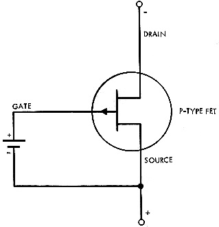
Fig. 3 - The basic circuit diagram of a p−type JFET amplifier.
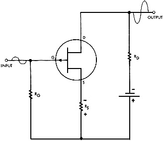
Fig. 4 - Typical characteristic curves of "p"−type FET.
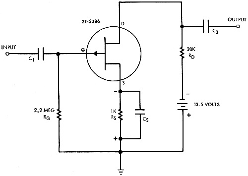
Fig. 5 - This simple amplifier circuit was built and tested.
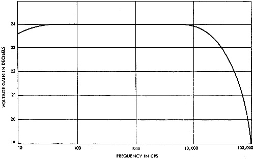
Fig. 6 - Measured frequency response of amplifier in Fig. 5. If the gate is now connected to the source lead, as shown in Fig. 1B, the flow of current through the device will be reduced. The natural resistivity of the p−type crystal will cause a voltage drop across the length of the p−type crystal bar between the source and the drain connections. This will result in the junctions between the n−type crystal in the gate regions and the p−type crystal in the main bar being reverse-biased. In other words, the gate areas will be positive with respect to the p−type crystal immediately adjoining them. As in any reverse-biased semiconductor junction, the areas on both sides of the junctions will be depleted of carriers (holes and free electrons) of electric current. This effect is exactly the same as when a junction diode is reverse-biased but the effect is now used in a little different way. With part of the narrow channel between the gate areas depleted of the current carriers, the electrical width of the current-carrying channel has been effectively decreased and therefore the conductivity of the narrow channel has been decreased. This will then decrease the amount of current flowing between the source and the drain. This effect can also be explained as the building up of an electric field at the above-mentioned junctions. This electric field is shown in Fig. 1B. Notice that it is wedge shaped, being wider toward the drain end of the device. This is because the potential between the gate region and the surrounding p−type crystal becomes greater nearer the drain end of the device. The arrangement shown in Fig. 1B would have very little practical application. However, a configuration somewhat nearer to the operational FET is shown in Fig. 1C. Here a positive bias potential is connected between the gate and the source. With this arrangement, an additional electric field appears at the internal junctions. This new electric field adds to the electric field already mentioned and a further reduction in source-to-drain current results. (The flow of electrons through the p−type FET is from drain to source; "conventional" current flow is in the opposite direction. - Editor) Technically the two fields are not exactly the same type (the electric field resulting from drain current being tangential to the junction and the electric field resulting from the external applied bias being normal to the same junction), but for all practical purposes they can be treated as being electric fields simply reinforcing each other. As the positive potential between the source and the gate is increased, the current through the device will decrease. It seems natural to expect that as the potential is further increased, a point would soon be reached where no current could flow in the channel. In practice, the channel current can be decreased to a very low value but it cannot be decreased to zero. It is now time to introduce the standard symbol for the p−type FET. In Fig. 2, the pictorial arrangement of the FET in Fig. 1C is replaced by the standard symbol for the FET but the external connections are the same. If the FET were constructed from a bar of n−type crystal and the gate regions made of p−type crystal, the operation would be the same except that the polarity of the voltages applied to the device and the direction of current flow would be reversed. The schematic symbol of the n−type FET is the same as the one shown except that the direction of the arrow in the gate connection is reversed. Both types of FET's are being produced commercially at the present time. It must be remembered that the physical configurations of the FET's on the market are much more refined than the example used here, but the basic construction principles are the same. Another of the differences between the FET and the conventional transistor can be demonstrated by referring to the circuit of Fig. 3. If the conventional junction transistor were connected in this way (considering the gate, drain, and source analogous to the base, collector, and emitter respectively of a p-n-p junction transistor), the transistor current would be at cut-off. In contrast, the FET circuit of Fig. 3 would have a conduction level determined by the resistance value of RS. The conventional junction transistor must be forward-biased at the input, resulting in very low input impedance, while the input to the FET is reverse-biased, giving it a very high input impedance. The resistor RS in the circuit of Fig. 3 allows the device to operate in the region over which the drain current can be controlled (increased and/or decreased). It is readily apparent that this is the same circuit arrangement that has been used to bias electron tubes for many years. The circuit action is the same as for electron tubes. With electron current flow from drain to source, a voltage drop of the polarity shown occurs across the resistor RS. As stated previously, this voltage acts as reverse bias across the gate-to-source junction and restricts the flow of drain current. Because you cannot have this bias without current flowing in the FET, the value of drain-current is determined by the value of the circuit components and the applied voltage. Very little or no voltage will be present across RG except that resulting from an input signal. When the input signal causes the gate to become positive, the reverse bias across the gate-to-source junction is increased and the current through the FET decreases. The voltage at the drain or output of the circuit will go in a negative direction. Conversely, with a negative input signal, reverse-bias of the gate-to-source junction is decreased and the source-to-drain current increases. With this condition, the voltage at the output becomes less negative or goes in a positive direction. Thus, the signal is amplified and undergoes a 180-degree phase shift as occurs in a vacuum-tube amplifier (common-cathode configuration) or in the conventional transistor amplifier (common-emitter configuration.) (In the case of an n−type FET, the similarity to a vacuum-tube circuit becomes even more obvious. The gate bias is negative, in this case, and the electron-current flows from the negative source to the positive drain. -Editor) Important Characteristics The characteristics to be described are some of those most commonly found on manufacturers' data sheets. It is important for the user of the FET to be familiar with them. Gate Cut-off Current (IGSS). This is nothing more nor less than the reverse-bias current across the junction between the n−type material and the p−type material of the FET. Because the source and drain leads both are connected to p−type crystal, these leads are connected together when measuring this current. With a p−type FET, the source and drain leads are connected to a negative potential and the gate to a positive potential. This will reverse-bias the junction. With this arrangement, the only current resulting will be the current due to minority carriers. As with any junction diode, this current will be determined by the characteristics of the crystal and by the temperature of the material. Because temperature can vary and the transistor characteristics are inherent, the amount of gate cut-off current will be determined mostly by temperature. At room temperature, this current will be in the low microampere region. As with any diode, the junction can be broken down if sufficient reverse-bias voltage is applied across it. Therefore, to prevent possible damage to the transistor the applied voltage is generally limited to 10 volts or less when measuring IGSS. Breakdown Voltage (BVDGO), Breakdown-voltage characteristics can best be explained by referring to Fig. 4. The curves are analogous to the IP versus EP curves of an electron tube and the IC versus VC curves of a conventional transistor. One of the main differences can be noted in that the VGS curves take a sharp upturn shortly above the 20-volt value of drain-to-source voltage. This point represents the breakdown voltage of the FET under a particular operating condition. Because the gate-to-drain junction is normally reverse-biased, the voltage between the drain and gate will exceed the voltage between the drain and source under normal operating conditions. For this reason, the drain-to-gate breakdown voltage largely determines the breakdown point of the FET. The drain-to-gate breakdown voltage (BVDG) is a constant value for a particular transistor and can be stated in relation to the other voltage values as follows: BVDG = BVDSX + VGS, where the subscript "X" denotes the value of drain-to-source breakdown voltage (BVDS) for a particular value of gate-to-source voltage (VGS). This relationship simply means that the reverse-bias be-tween the gate and source will cause the FET to go into a voltage breakdown condition with a smaller source-to-drain voltage than would otherwise occur. This can be verified by examining the curves of Fig. 4. As the value of VGS goes in a positive direction, the breakdown voltage occurs at a smaller value of VDS. It should be obvious that if the FET is to be used as an amplifier, it must be operated in the region below the breakdown voltage at all times. Also, the value of the applied voltage must always be less than the value of BVDG given on the data sheet for any particular FET. Saturation Drain Current (ID(ON)). This is the symbol for the amount of drain current at zero gate-to-source voltage at a specified value of source-to-drain voltage. With this condition, the current in the channel between the gate region is determined only by the electric field developed in the channel by reason of the voltage drop across the crystal bar between the source and gate regions. The value of ID(ON) decreases with an increase in temperature because silicon has a positive temperature coefficient causing a larger voltage drop at higher temperatures with the same value of drain current. ID(ON) is measured in the saturation or pinch-off region of the characteristic curve. Pinch-off Current (ID(OFF)) is the current flowing in the FET with a specified value of reverse-bias applied to the gate-to-source terminals. This reverse-bias is usually in the region of 5 volts which is considerably more than enough to bias the FET below the linear operating region and near the drain current cut-off point. As stated previously, the current through the transistor cannot be limited to zero by reverse-biasing the gate-to-source regions. Consequently, ID(OFF) as given on a data sheet is actually the value of drain leakage current that the manufacturer guarantees to be the maximum under specified operating conditions. This value is usually only a few microamperes of current and this value varies little with temperature. Those persons who were reared on vacuum-tube theory will feel pleasantly at home working with the FET. The circuit design procedures for the vacuum tube are largely applicable to the FET. The basic amplifier shown in Fig. 5 was designed and constructed in the electronics labs at General Dynamics, Fort Worth. This circuit was built to illustrate the simplicity of designing and operating FET amplifiers. We were also interested in checking the performance of a basic amplifier employing a fairly inexpensive field-effect transistor. Basic Amplifier Circuit The data sheet for the 2N2386 transistor gives a guaranteed minimum value of BVDGO of 20 volts. The voltage source of 13.5 volts used in this circuit is then safely below this value. RG was selected so that very little shunting of the input signal would result; therefore giving a high value of circuit input impedance. RS determines the operating point of the FET while RD is the load resistance whose value largely determines the amplitude of the output signal voltage. As in any amplifier, the capacitance values are determined primarily by the lowest frequencies that are to be amplified in the circuit. The input impedance was found to be extremely high at signal input frequencies below 10 kc. Above this value the input impedance decreased considerably due to the shunting effect of the input capacitance of the FET. However, the input impedance still remained considerably higher than that for conventional transistor amplifiers. The manufacturer lists the input impedance of the 2N2386 above 3 megohms at frequencies up to 1 kc. The voltage gain was found to be approximately 24 db at frequencies up to 10 kc. and down only 1 db at 30 kc. The curve of Fig. 6 shows the measured frequency response for this amplifier. The small decrease in gain at low frequencies was a result of insufficient bypass and coupling capacitance at the lowest frequencies. The input impedance and frequency response can be improved considerably with more refined circuit design. In fact, circuits have been designed with input impedance of at least 200 megohms and with good frequency response up to and above 10 mc. Another major advantage of the FET is low noise characteristics. In general, the FET has proven to have lower inherent noise than either vacuum tubes or conventional transistors. Further drain current and drain-to-source voltage changes have proven to have little effect on the amount of noise generated in the circuit. These advantages should cause the FET to enjoy a much wider application in the future, especially where high input impedance is required.
Posted December 5, 2022 |
|