Computer-Designed PC Boards
|
|
Even in the early days of "computer-designed" printed circuit boards, the software was sophisticated enough to take a circuit net list and perform a rudimentary auto-routing all of metal traces, component solder pads and through holes, using a set of defined design rules for line width and spacing, component size, number of layers, etc. Manual tweaking was usually needed after the initial run, but even today, especially for high frequency PCBs, some manual adjustment is needed to help ensure first-pass success of a layout. According to author Bauer, as many as 22 layers had been accomplished at the time of the article's printing in 1969. Numerically controlled machines were already being used to produce artwork and drill through holes. What kinds of computers did the heavy computations in the day? "A 12 x 12 inch board with 50 thousandths of an inch grid requires 120,000 bytes of memory. This memory capacity is supplied by a medium- to large-scale computer." Your smartphone can do much more today than a medium- to large-scale computer could then. Computer -Designed PC Boards By J. A. Bauer / Advanced Digital Design Manager Missile and Surface Radar Division, RCA How and when computers should be used to produce artwork for PC boards. Computer hardware and programming are described. Military and commercial electronic systems are becoming more complex as performance requirements increase. Through use of low-cost digital integrated circuits these requirements can be met economically. Electrical components can be reliably packaged and interconnected on multilayer printed-circuit boards. Interconnections between component leads and conducting-board layers are made by plated-through "via" holes.
The author was graduated from VPI in 1946 and has attended advanced courses at the University of Pennsylvania and UCLA. He holds two patents in the electronics field and has published papers on digital calendar clocks and computer-controlled telemetry systems. Critical to the production of printed-circuit boards is the artwork required for each layer of conductors. The artwork must contain all interconnecting information in precise and accurate form on film or glass transparencies to expose the copper layers for subsequent etching to form individual conductors. Printed circuits can range from a simple, single-sided board with a few components and connections to complicated boards with hundreds of components and thousands of interconnecting copper paths. Manufacturing artwork for the simple board is easily laid out and checked by hand, but the multilayer board poses problems in component placement, lead routing, and multilayer circuit tracing. Since multilayer boards are extremely complicated, they are better handled by the high-speed digital computer which is capable of large-scale processing without error. Two avenues of approach have proved practical and are being concentrated on within the printed-circuit industry. One is computer-aided design where the computer is used as a bookkeeping and drafting tool. Entered data is displayed by way of a cathode-ray tube where it can be controlled by the designer. The other is design automation, which makes use of sophisticated computer software programs to make decisions, such as where to place components, how to route wire paths, and how to test the finished board. Both systems have one thing in common - the requirement for a complete description of the printed-circuit board. Within the computer memory the size, shape, and detail geography of the board must be laid out. The memory must also include a pattern of allowable interconnection points for the components and connectors and a grid system for the possible paths of interconnecting wires. At this point it becomes obvious that a set of printed-circuit boards for any one job should have common physical dimensions and placement grid, not only to reduce the task of the packaging and layout designer, but also to reduce the effort in entering this data to the computer. Since this is the practice whether a computer is used or not, the computer presents no limiting factor. Although both computer-aided design and design automation are tools in printed-circuit design, this article will concentrate on design automation because of its rapid decision-making capability in addition to bookkeeping and, therefore, its faster operation in preparing large-scale artwork for PC boards. The computer can't cheat, lie, or steal because it is constrained to operate within its program. It is not capable of inventing new methods of solution to a problem as the program progresses. Therefore, it is desirable that the computer program take into account as many subtle factors as possible in order to achieve competitive operation with the human designer's layout. For this reason, computer programs are difficult and time consuming to write and are considered to be a major effort. Design Automation A typical printed-circuit artwork program consists of a memory bookkeeping section, an interconnection checking section, a component placement section, a wire path routing section, and a magnetic tape output to a numerically controlled artwork generator. In addition to the artwork program, drill point location and test programs may also be prepared to drive numerically controlled drills and test machines. Inputs to the system are the board configuration and the interconnection list of the components. A flow diagram of a typical design automation system is shown in Fig. 1.
Fig. 1 - Flow diagram of an automated printed-circuit artwork system. After the board configuration and the interconnection list have been entered either by means of keypunched cards or other mechanisms, the computer is programmed to check the interconnection list for completeness. If an error has been made in transcribing from the logic diagram or in making the logic diagram, the computer produces an error list which is typed out and fed back to the designer. A typical check run by the computer includes completeness of wiring path; a wiring path must terminate at connections. After check of the manually generated data, the computer is programmed to place components so they will be interconnected as simply as possible. The usual placement criterion is to reduce to a minimum the length of connections while taking into account the available channels for interconnections in each direction. For instance, if the board geometry dictates that only two wiring channels are available between components in the X direction and four wiring channels are available in the Y direction, this factor should be considered in preparing the computer program so that component placemen t is made with more wires available in the Y direction. Component placement is done by the placement algorithm. The computer rapidly assembles the total wiring length, then re-arranges components and checks wiring lengths again to achieve a minimum total wire length. An additional constraint can be made to eliminate excessively long interconnection paths, particularly for critical signals. Because the computer can make multiple placements and wiring length calculations very quickly, several thousand alternate placements can be made before the optimum placement is selected. Routing Program Once an optimum placement is selected, a routing program is initiated. In this phase, the computer attempts to interconnect components in accordance with the interconnection list given to it by the logic designer. At this point, it is programmed to operate like a mouse running through a maze from start to end of the interconnect - it must avoid components, wiring pads, and previously laid out wiring paths. This is called the routing or maze-runner program. However, unlike the mouse in a maze, there are usually many alternate paths available to make an interconnection. The interconnection may stay on one layer of the printed-circuit board or it may be allowed to go from layer to layer. It may be preferable for it to follow one direction over another in order to avoid blocking interconnections which will be made later. Also its possible path may be so long around other components and wires that it would be preferable to reserve the path for a different laver on the board where the path would be shorter. All of these various constraints should be taken into account when setting up the routing program.
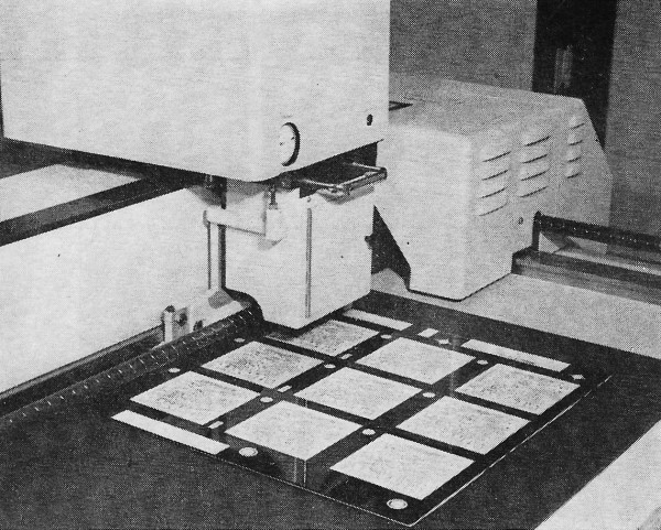
Fig. 2 - Numerically controlled artwork generator producing the artwork for a group of nine identical PC boards.
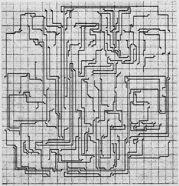
Fig. 3 - Example of computer-generated artwork in which most of the lines are in the Y, or vertical-axis, direction. It has been our experience that as the computer program is made more sophisticated in this area, better performance is achieved, thereby increasing the number of interconnects per layer of artwork. Most of the industry's efforts are concentrated on improving computer programs because the more factors that can be taken into account in the program, the more efficient the artwork can be made. The current state of the art indicates that human intervention is still desirable in order to reduce the number of layers in densely packaged printed-circuit boards. However, it is also highly desirable to have all of the information included within the computer so that directions to the numerically controlled artwork generator, drill, and tester can include all data. A typical example of computer routing for a densely packaged board mounting one-hundred integrated circuits may take two hours of computer time and produce eight layers of signal wiring. With manual intervention, the number of layers may be reduced to six. A prototype multilayer board may be made with the computer program, then changes to the interconnection and additional edited reduction of printed-circuit signal layers may be made for the production boards along with any additional changes determined by prototype test. As many as 22 layers have been successfully interconnected with printed-circuit techniques, indicating the current success of this method. The programming complexity required by computer layout of multilayer printed-circuit boards indicates that this service requires a large investment. Therefore, it is usually more economical to utilize available programs from one of the large printed-circuit producers who will accept circuit or logic diagrams or interconnection lists rather than requiring each engineer to start from scratch to generate computer programs effective enough to prepare artwork. The engineer and packaging designer should then consider very carefully whether it would be more efficient to manually layout his densely packed printed-circuit boards or utilize one of the available services of the printed-circuit manufacturer. One of tile items to be taken into account is the number of errors produced by the many steps of manual placement and layout of thousands of interconnects, and the resultant recycling of artwork to correct mistakes compared to the relatively error-free operations of design automation. The designer should also consider the time savings of design automation caused by rapid computer operations. Making the Artwork Once the placement and interconnection routing have been accomplished, a magnetic tape is prepared by the computer to drive a numerically controlled artwork generator. Fig. 2 shows an artwork generator in operation. It is possible to prepare artwork to within 0.0004-inch accuracy with this machine made by the Gerber Scientific Co. Notice that multiple artwork is being prepared on one master so that a group of nine identical printed circuits can be etched at one time. The machines, currently used by RCA, drive a light head which exposes the film master on the table. Two machines are available to produce automated artwork for printed-circuit boards, integrated circuits, and for shadow masks for color-TV picture tubes. An example of computer-generated artwork is shown in Fig. 3, which is a sketch of one of two layers of a multilayer board prepared for checkout before final artwork is made. The typical layouts for a pair of adjacent layers results in artwork in which most of the lines in one layer run at right angles to most of the lines in the next layer. This is an important programmed portion of the computer-generated artwork because a single X (horizontal-axis) connection allowed to cross a layer with most of the connections in the vertical-axis (Y) direction could block paths of many wires in that layer, thereby limiting the wiring density of the layer pair. Other, more subtle, effects can occur when attempting to program multiple-layer printed-circuit cards. For instance, it is desirable to vary the interconnection path selection depending on which edge of the board is being wired in order to make maximum use of the board edge. It is also desirable to anticipate the result of using via holes by the computer program since it may be more efficient to reserve them for manual additions.
Fig. 4. Using automatic equipment to run continuity and short-circuit tests on completed printed-circuit boards, Considering the above information, the circuit-card designer may feel that designing an efficient automated artwork program is specialized and expensive. This is true. At least several man-years of professional programmer's time are required to prepare the computer software which is competitive with manual layout methods. There is no simple mathematical proof for any of the placement and routing algorithms used. They must be invented and tested by practice with actual printed-circuit boards to gain sufficient experience in predicting performance. Since the exact number of layers to be produced by the automated program is difficult to predict for densely packed boards, it is desirable to have a manual editing program to take advantage of human inventiveness and visualization which the computer program cannot have built in. As an example of performance currently obtainable, a circuit board with 800 interconnecting wires may be produced automatically in eight layers and, with additional manual editing, could be reduced to six. The Equipment Involved The equipment involved in automated artwork should also be considered. The limiting factor of the computer used to design large multilayer printed-circuits is the memory capacity. Each grid point capable of accepting a wiring path must be entered in memory. A printed-circuit board with dimensions of 6 x 6 inches and a grid of 50 thousandths of an inch requires at least 30,000 bytes of memory. A board with 25 thousandths of an inch grid requires 120,000 bytes of memory. Alternatively, a 12 x 12 inch board with 50 thousandths of an inch grid requires 120,000 bytes of memory. This memory capacity is supplied by a medium- to large-scale computer. The computer. when properly programmed, is capable of preparing tapes driving numerically controlled artwork generators. These may be of the high-speed, medium-accuracy cathode-ray-tube type or the slower speed but highly accurate electro-mechanical plot board. These are the two major hardware components required for automated artwork preparation. Although it is possible to rent service on these devices, most of the producers making printed-circuit boards have them available in-house. RCA, Moorestown, has available on its Spectra 70/55 computer, a memory capacity of 262,000 bytes. Two highly accurate Gerber photoplotters are also available. Each completed circuit board must be tested to assure quality. At our printed-circuit facility, automated continuity and short-circuit tests are run by the DIT-MCO tester shown in Fig. 4. Because of the large investment in time and equipment, design automation for multilayer printed-circuit boards will be most effectively used as a service from the printed-circuit manufacturers rather than as separate programs generated by each of the designers. This currently available service reduces artwork production time and cost and should be considered in choosing PC manufacturers. Automated artwork can be most advantageously applied to more complicated, densely packed integrated-circuit boards requiring multiple layers of interconnection. Single-layer boards are currently laid out more efficiently by manual means. One of the reasons is that as complexity increases so does the chance for making errors in manual artwork. These errors are difficult to catch and only one error in an 800 interconnect board requires modifications of the board. Future Developments Automated artwork is one of the items required not only for efficient production of multilayer printed circuits but also for large-scale integrated circuits. An advance in one of these technologies will also benefit the other. The state of the art is rapidly improving because of the newness of the field and the current availability of all the tools, such as computers and plotters. The limiting factor advancing the state of the art is the inventiveness of programmers preparing software. Certainly in the future computers will produce more calculations per dollar and plotters will become faster and more accurate, still the capability of automatic artwork will depend on the capabilities put in by the programmer. In addition to solving the placement and routing problems, the programmer will be adding wiring rule calculations for solving reflection and cross-talk caused by interconnections of high-speed circuits. Moreover, minimum test specifications and a program to define and locate logic errors will also be added in the future. Programs are available to check the logic by simulation and to prepare waveform and timing checks. When these are integrated into the over-all printed-circuit artwork preparation, the engineer will be assured of the proper logic operation in accordance with his design as well as efficient artwork production and test.
Posted October , 2017 |
|