The Future of Thin-Film Active Devices
|
|
When Charles Feldman published this article on thin-film transistors (TFTs) in a 1964 issue of Electronics magazine, he had no idea that the devices would eventually play a major role in liquid crystal displays (LCDs) in everything from wristwatches to large screen television and computer displays. Materials and fabrication techniques have evolved considerably since 1964, but the fundamentals remain the same. Other than LCDs and some solid-state sensors, I am not familiar with any other applications that are heavy users of TFT technology. This 2016 paper titled, "Review on thin-film transistor technology, its applications, and possible new applications to biological cells," gives a little historical perspective and a comparison of CMOS versus TFT. The Future of Thin-Film Active Devices
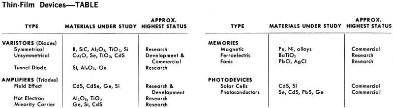
Fig. 1 - Frequency Modulated oscillator, slightly less than an inch wide. Survey of potential applications of thin-film field-effect devices as amplifiers, varistors and current limiters By Charles Feldman, Melpar Inc., Falls Church, Va. Author's Prediction Systems containing the film device concepts discussed here will probably be in operation within three to five years. This in itself is remarkable, considering that a few years ago it was believed impossible to form useful thin-film active devices. This viewpoint has gradually changed through the efforts of numerous people in various laboratories. Many effects suitable for film devices are being explored. Effects such as tunneling and hot-electron emission hold promise, as well as other phenomena listed in the table. It thus appears that thin-film electronics will soon outgrow the laboratory and take its place in the electronics industry. At present, the principal value of thin-film electronics appears to lie where environment conditions preclude the use of conventional electronics. Recent radiation tests have indicated that thin-film active devices, as well as thin-film passive devices, offer considerably more resistance to gamma rays than conventional components.1 There is little question that thin-film devices, which are composed of polycrystalline material and operate on majority-charge-carrier concepts, will be generally more radiation resistant than conventional single-crystal devices. It is becoming increasingly clear, however, that present thin-film devices represent merely a beginning of thin-film electronic technology." Under study at various laboratories throughout the world are numerous types of physical effects, many of which will lead to practical film devices in the ensuing years. Some of these possible devices are listed in the table, which is by no means complete, but illustrates the large variety of materials and effects under various stages of development. The physical effects leading to the listed devices, of course, already exist. It is only a matter of time before all or most of the devices in the list are developed into useful devices.
Fig. 2 - Definitions of thin-film transistor parameters.
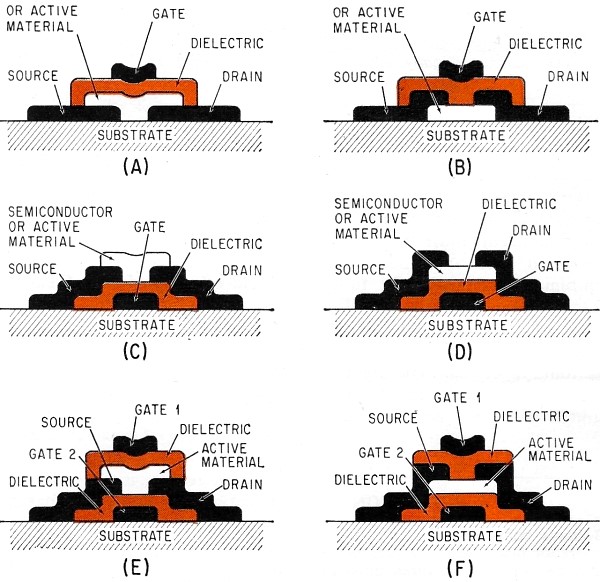
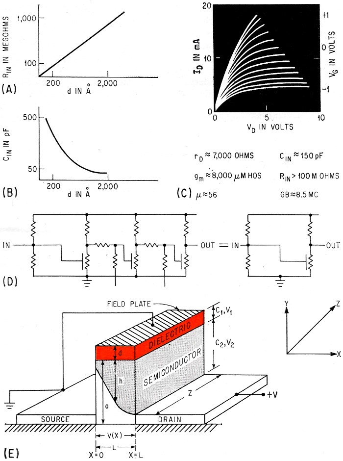
Fig. 3 - Field-Effect Device structures: simplest structure for automatic deposition (A), most frequently used at Melpar; structure (B) is used when semiconductor layer is to be treated prior to device completion; (C), reverse deposition order of (A) with exception of source-drain electrodes, used as first step of structure (E); (D), exact reverse deposition order of (A), no particular advantage except when forming double gates as in (F); (E and F), same as structures (C) and (D) respectively, with addition of dielectric and second gate. The second gate increases the overall gain of the device, but is more difficult to fabricate. The transformation of the effects and materials under study into practical components must, however, be considered only a prelude to the thin-film electronics of the future. Materials listed in the table will be combined in various sophisticated geometries to produce complete electronic functions. The ability to form complete electronic functions through geometry may be considered as the key to advanced electronics. The use of this key in two thin-film devices, a field-effect transistor and a varistor, will be discussed. Field-Effect Devices - Field effect, or the variation of current in a material by the application of a transverse electric field, may be used as a variable resistor, a variable capacitor or a purely amplifying device depending on the configuration of the layers. An excellent example of the use of a field-effect as a variable resistor is shown by the application of distributed parameter concepts in an f-m oscillator. The circuit was designed to use a commercial transistor as the amplifying device. The essential element in this circuit consisted of successive layers of germanium, silicon monoxide and aluminum forming a distributed capacitor. The germanium plate was shaped, in the plane of the substrate, in a logarithmic taper to achieve an impedance match to the amplifying transistor. The resistance of this germanium film could be modulated by an electric field applied between it and the top aluminum plate. Other semiconducting materials, such as CdS and CdSe, may also be used in place of this germanium film. This circuit (Fig. 1) has been described in detail elsewhere." The use of active film layers combined with distributed parameter networks will reduce the number of individual circuit components, thus resulting in greater circuit reliability. The influence of geometry on an amplifying field-effect element is shown in Fig. 2, and other variations of the device structure in Fig. 3. An enlarged photograph of the front and back view of an array with 81 devices per square inch is shown in Fig. 4. Note that the gate electrodes (small circles) as well as the source and drain electrodes may be connected by a straight line. Figure 2 shows how electrical parameters such as transconductance, dynamic resistance and gain-bandwidth are related to sample geometry. The behavior of input capacitance and resistance on the thickness of the dielectric layer is shown in Fig. 5A and 5B. The frequency response of the device is determined through the gain-bandwidth product. The ratio of channel spacing to charge carrier mobility (L/μ), which determines the transit time of the carriers, in addition to the total capacitance of the sample, limit the frequency response. It is believed that, with the presently attainable film mobilities and channel spaces, frequencies of over 100 Mc can be achieved. Performance - As shown in Fig. 2, transconductance (gm) is directly proportional to the width of the source-drain electrodes (Z) and inversely proportional to the channel spacing (L). The electron mobility (μo), which appears in the expression for gm, is also dependent on the thickness of the semiconductor layer. Thus, any desired transconductance can be achieved with proper geometry and available space. Recently, tests have been made in this laboratory in which five similar devices were connected together simulating a width, Z, five times larger. The resulting characteristics are shown in Fig. 5C. The individual units had nearly identical characteristics. Transconductance values of each sample was in the vicinity of 1,500 μmhos, and the parallel arrangement, yielded a transconductance of 8,000 μmhos. Similar high transconductance values were also obtained by forming a single unit with a source-drain width of 500 mm, five times the single units described above, and a 0.013-mm channel spacing. Values of transconductance up to 20,000 μmhos were achieved in this manner; however, appreciable hysteresis was noted in the oscilloscope displays for devices with transconductance greater than 10,000 μmhos.
Fig. 4 - Front and Back views of array with 81 devices per sq cm.
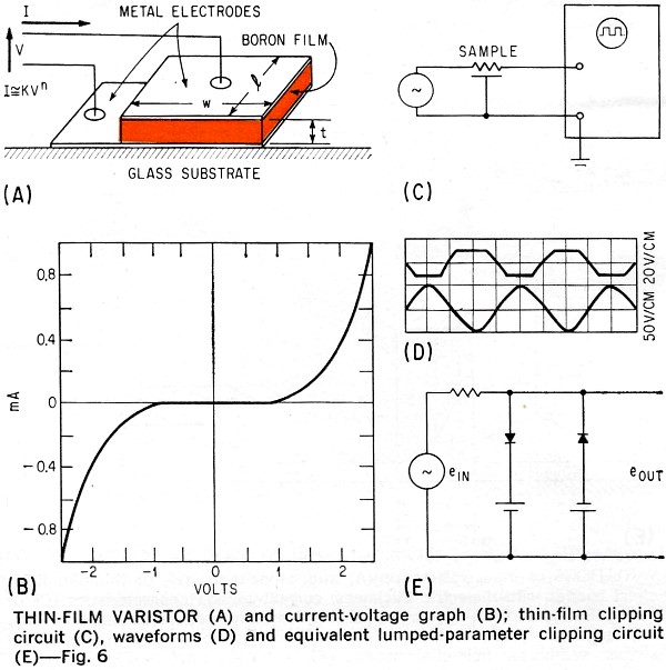
Fig. 5 - Variations of input resistance (A) and capacitance (B) of thin-film field-effect triodes with dielectric thickness; current-voltage characteristics (C) of five CdSe field-effect devies in parallel; resistance-coupled amplifier (D), reduced from three devices and nine resistors to one device and three resistors; self-biased field-effect device (E), a current limiter. The ability to choose the desired electrical properties through the choice of geometry enables one to simplify electronic circuits. One example of this simplification (Fig. 5D) illustrates the reduction in numbers of devices, components and connections in a resistance coupled amplifier, achieved by making the device width (Z) three times larger. Device characteristics can, of course, be altered in crystalline transistors as well as electron tubes; however, nowhere is the ability to alter easier than in vacuum-deposited film circuits where a change in masks during deposition will result in the required modified device parameters. The amplifier in Fig. 5D was built, and had a flat response to 100 kc. The voltage gain was about 1,000; however, no degenerative feedback was used as is commonly done with direct-coupled amplifiers. An attractive application of field-effect devices is their use as current limiters.4 In a current limiter, the source and gate are connected making the device into a two-terminal one as in Fig. 5E. The effect of connecting the source and gate together is to essentially reverse-bias the device, which causes a depletion layer to be created in the semiconductor film. As the applied voltage increases, the effective conducting path decreases (depletion layer increase) until "pinch-off" is reached and the constant-current condition is attained. The ultimate value of the current depends on the device with (Z). It is easy to imagine many other variations in geometries that illustrate the versatility of field-effect phenomena in electronic circuitry. The examples given, however, illustrate the potentials of the device and the versatility of thin-film techniques. As fabrication techniques and material knowledge improves, device parameters will improve and applications will become more numerous. Device cost, even in laboratory quantities, looks extremely promising. Thin-Film Varistors - Varistors or nonohmic, two-terminal, solid-state devices (diodes) have been under exploration for many years." Layered or film varistors, such as selenium and copper-oxide rectifiers, were among the first solid-state components commercially available. As indicated in the table, both symmetrical and nonsymmetrical varistors are being studied in thin-film form. Research is being emphasized on phenomena such as tunnel effects, field effects and barrier effects. Thin-film varistors using each of these phenomena have been fabricated in this and other laboratories. There is no question that each effect and corresponding device will play its role in the thin-film electronics of the future. Varistors can be tailored to meet specific electronic requirements in precisely the same manner as the field-effect devices described above. An example is easily found in a new type of symmetrical varistor being explored in this laboratory. This varistor consists of deposited layers of metal, boron, and metal respectively. The metal-film electrodes are usually formed of aluminum; however, other metals such as gold appear to give equal results. The boron deposition is carried out by an electron beam. The properties of a typical sample are shown in Fig. 6A and 6B. The device has characteristics similar to silicon carbide bulk varistors and may consequently be used in similar fashions." The physical explanation of such non-linear current-voltage curves is, at the moment, not clear. It appears from experimental work that an extremely pure, amorphous, boron film is necessary. Considerably more research in the physics involved will be required to completely explain the nonlinear characteristics of the device. Obviously, the electrical properties of this varistor can be controlled by geometry. The area of the plates determines the total current flow, while the boron thickness controls the voltage operating point.
Table 1 - Thin-Film Devices
Fig. 6 - Thin-Film Varistor (A) and current-voltage graph (B); thin-film clipping circuit (C), waveforms (D) and equivalent lumped-parameter clipping circuit (E). Distributed parameter techniques may be employed to advantage in thin-film varistors, If a resistive layer is substituted for one of the metal plates or electrodes, a three-terminal device is obtained. Such a device may be used as a clipping circuit, as in Fig. 6C to 6E. In this clipping network, the three-terminal device parameters are controlled by the thickness and area of the metal resistive layer as well as the area and thickness of the boron layer. A design engineer must thus specify, length to width ratio, ohms per square, area and device thickness to obtain "clipping" at the required voltage. Conclusions - Circuits using thin-film active devices are currently being evaluated in the laboratory. These circuits will be fabricated on automatic deposition equipment, which uses a phonograph record changer concept for mask and substrate pallets and an electron beam source for deposition. Initial tests with this equipment have proven the feasibility of automatically depositing complete circuits on a production basis. The author acknowledges the efforts of all the members of the Physical Electronics Laboratory. The work of Herbert Wilson and William Gutierrez on active devices and Charles Gane on device circuits is particularly appreciated. The support of the Bureau of Naval Weapons on all phases of this work is gratefully acknowledged. References (1) R. W. Marshall, Microelectronic Devices for Application in Application in Transient Nuclear Radiation Environments, Proceedings of East Coast Conference on Aerospace & Navigational Electronics, IEEE, Baltimore, Oct. 22, 1963. See also: Aviation Week and Space Technology, p 93, Aug. 17, 1963. (2) For a state-of-the-art review see: "Integrated Circuits, Technical Review & Business Analysis," by Graduate Students of the Harvard Business School, Integrated Circuits Associates, P. O. Box 131, Cambridge, Mass., 1963. (3) H. E. Culver and C. E. Gane, Proc IEEE, 51, p 1,034, 1963. See also: Electronics, p 24, Oct. 12, 1962. (4) W. A. Gutierrez, H. L. Wilson. "An Analysis of the CdSe Thin-Film Triode as a Current Limiter," to be published. (5) F. R. Stansel, "The Characteristics and Some Applications of Varistors," Proc IRE, 39, p 342, 1951. (6) See for example, L. D. Kovack and W. Comley, IRE Trans. on Electronic Computers, EC-9, p 496, Dec. 1960.
Posted July 24, 2023 |
|
")