A/D Converter Calculations for RF Applications |
|||||||||||||||||||||||||||||||||||
|
These equations predict the RF electrical performance of an Analog-to-Digital Converter (ADC, A2D, A/D converter, etc.). Since A/D converters are often the last stage in a receiver chain, it is extremely useful to be able to predict the contribution for noise figure, signal-to-noise ratio, power levels, etc., since those values are needed for a complete cascade analysis. Lots of variations on the equations can be found across the Internet, so I have endeavored to reduce them to a few most common quantities. Calculations for dynamic range vary considerably amongst sources, so they are not presented here. It is best to consult device datasheets when possible for specific values. Note: The following equations
are valid for pure sinewave inputs with no DC
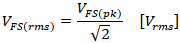
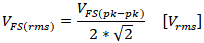
Full Scale Voltage & Power Power of a sinewave is calculated based on the root-mean-square (rms) value of the full-scale voltage. VFS(rms) calculated from the peak (pk) input voltage is:
Using the peak-to-peak voltage (pk-pk):
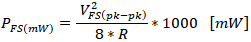
Full-scale input power in units of milliwatts (mW) based on full-scale peak-to-peak input voltage is:
Full-scale input power in units of dBm is:
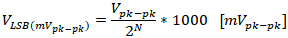
Quantization Levels of an Analog-to-Digital Converter (ADC) The value of a 1-bit (LSB, aka "q" level) voltage step anywhere between 0 and N bits for an N-bit ADC is:
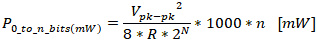
The value of an n-bit voltage step anywhere between 0 and N bits for an N-bit ADC is:
Because decibel units represent a logarithmic and not linear relationship between of number of ADC bits ("n") and power level, a simple multiplication of "n" or "n2 - n1" times some fixed power reference value does not work. Instead, you must calculate the value in watts (or mW, nW, etc.) for each number of bits using the voltage at each level, then conversion to dBm units can be made for an absolute value at each bit count:
The difference in Pn1(dBm) and Pn2(dBm) is expressed in units of dB as follows:
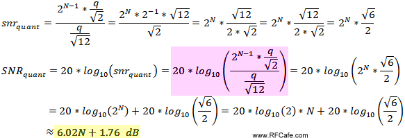
Signal-to-Noise Ratio (SNR) of an Analog-to-Digital Converter (ADC) Most sources give the ideal quantization-based signal-to-noise ratio (SNR) equation as 6.02*N + 1.76 dB (yellow highlight below). A little more research turns up the source of that equation (purple highlight below). Here, I show the steps between purple and yellow, using common rules of logarithms and rules of exponents.
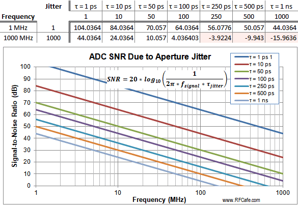
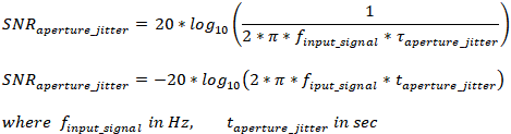
It might be best to use the worst case of either SNRclock_jitter or SNRquant for system budget planning. Datasheets often provide SNR information, which should be used instead of any generalized equations. Noise Figure of an Analog-to-Digital Converter (ADC) Probably the most difficult equation to find for an ADC is for noise figure (NF), which is typically the last component in a cascade calculation of a receiver chain. My source for the equation is a Texas Instruments (TI) document authored by Mr. Tommy Neu (it also appeared in MWJ). You need the SNR value either from the ADC datasheet or from the above equation is required. Noise spectral density (NSD) is also needed, so its equation is provided as follows. NSD units are formally W/Hz or, equivalently, V/√Hz; however, the equations are provided without units because of the manner in which bandwidth is absorbed into them in these simple forms.
where:
Finally, the noise figure (NF) is calculated, where kTB is −174 dBm/Hz:
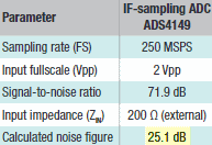
Example
fsample_rate = 250 Msps N = 16 bits Vpk-pk = 2 V SNRfull_scale = 71.9 dB kTBT=290K,B=1_Hz = -174 dBm R = 200 Ω
Updated August 16, 2019 |
|||||||||||||||||||||||||||||||||||


 ,
,