Module 21 - Test Methods and Practices |
||||||||||||||||||||||||||||||||||||||||||||||||||
|
Module 21 − Test Methods and Practices
Pages i , 1−1, 1−11, 1−21, 2−1, 2−11, 2−21, 2−31, 2−41, 3−1, 3−11, 3−21, 3−31, 4−1, 4−11, 5−1, 5−11, 5−21, 5−31, AI−1 to AI−3, Index
Always check the condition of the test set batteries by disconnecting the test set power cord, placing the POLARITY switch in the PNP position and placing the Function switch first to BAT.1, then to BAT.2. In both BAT positions the meter pointer should move so as to indicate within the red BAT range.
BETA MEASUREMENTS. - If the transistor is to be tested out of the circuit, plug it into the test jack located on the right-hand side below the meter shown in figure 2-4. If the transistor is to be tested in the circuit, it is imperative that at least 300 ohms exist between E-B, C-B, and C-E for accurate measurement. Initial settings of the test set controls are as follows:
1. Function switch to BETA
2. POLARITY switch to PNP or NPN (dependent on type of transistor under test)
3. RANGE switch to X10
4. Adjust METER ZERO for zero meter indication (transistor disconnected)
Note: The POLARITY switch should remain ofF while the transistor is connected to or disconnected from the test set. If you determine that the beta reading is less than 10, reset the RANGE switch to X1 and reset the meter to zero.
After connecting the yellow test lead to the emitter, the green test lead to the base, and the blue test lead to the collector, plug the test probe (not shown) into the jack located at the lower right-hand corner of the test set. When testing grounded equipment, unplug the 115 vac line cord and use battery operation. The beta reading is attained by multiplying the meter reading times the RANGE switch setting. Refer to the transistor characteristics book provided with the tester to determine if the reading is normal for the type of transistor under test.
ELECTRODE Resistance MEASUREMENTS. - Connect the in-circuit probe test leads to the transistor with the yellow lead to the emitter, the green lead to the base, and the blue lead to the collector. Set the Function switch to the OHMS E-B position, and read the resistance between the emitter and base electrode on the center scale of the meter.
To read the resistance between the collector and base and the collector and emitter, set the Function switch to OHMS C-B and OHMS C-E. These in-circuit electrode resistance measurements are used to correctly interpret the in-circuit beta measurements. The accuracy of the BETA X1, X10 range is ±15 percent only when the emitter-to-base load is equal to or greater than 300 ohms.
Ic MEASUREMENTS. - Adjust the METER ZERO control for zero meter indication. Plug the transistor to be tested into the jack or connect test leads to the device under test. Set the PNP/NPN switch to correspond with the transistor under test. Set the Function switch to Ic and the RANGE switch to X0.1, X1, or X10 as specified by the transistor data book for allowable leakage. Read the amount of leakage on the bottom scale, and multiply this by the range setting figure as required.
DIODE MEASUREMENTS. - Diode qualitative in-circuit measurements are attained by connecting the green test lead to the cathode and the yellow test lead to the anode. Set the Function switch to DIODE IN/CKT and the RANGE switch to X1. (Ensure that the meter has been properly zeroed on this scale.) If the meter reads down scale, reverse the POLARITY switch. If the meter reads less than midscale, the diode under test is either open or shorted. The related circuit impedance of this test is less than 25 ohms.
2-11 PRECautionS. - Transistors, although generally more rugged mechanically than electron tubes, are susceptible to damage by excessive heat and electrical overload. The following precautions should be taken in servicing transistorized equipment:
1. Test equipment and soldering irons must be checked to make certain that there is no leakage current from the power source. If leakage current is detected, isolation transformers must be used.
2. Ohmmeter ranges that require a current of more than 1 milliampere in the test circuit are not to be used for testing transistors.
3. Battery eliminators should not be used to furnish power for transistor equipment because they have poor voltage regulation and, possibly, high ripple voltage.
4. The heat applied to a transistor, when soldered connections are required, should be kept to a minimum by using a low-wattage soldering iron and heat shunts (such as long-nose pliers) on the transistor leads.
5. All circuits should be checked for defects before a transistor is replaced.
6. The power should be removed from the equipment before replacing a transistor or other circuit part.
7. When working on equipment with closely spaced parts, you will find that conventional test probes are often the cause of accidental short circuits between adjacent terminals. Momentary short circuits, which rarely cause damage to an electron tube, may ruin a transistor. To avoid accidental shorts, a test probe can be covered with insulation for all but a very short length of the tip.
Electrostatic Discharge Sensitive (ESDS) Care
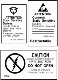
Devices that are sensitive to electrostatic discharge (ESD) require special handling. You can readily identify ESD-sensitive (ESDS) devices by the symbols shown in figure 2-5. Static electricity is created whenever two substances (solid or fluid) are rubbed together or separated. The rubbing or separating of substances causes the transfer of electrons from one substance to the other; one substance then becomes positively charged, and the other becomes negatively charged. When either of these charged substances comes in contact with a grounded conductor, an electrical current flows until that substance is at the same electrical potential as ground.
2-12
Figure 2-5. - Warning symbols for ESDS devices.
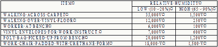
You commonly experience static build-up during the winter months when you walk across a vinyl or carpeted floor. (Synthetics, especially plastics, are excellent generators of static electricity.) If you then touch a doorknob or any other conductor, an electrical arc to ground may result, and you may receive a slight shock. For you to experience such a shock, the electrostatic potential created must be 3,500 to 4,000 volts. Lesser voltages, although present and similarly discharged, normally are not apparent to your nervous system. Some typical measured static charges caused by various actions are shown in table 2-1.
Table 2-1. - Typical Measured Static Charges (in volts)
Q-10. At approximately what minimum voltage potential should you be able to feel an electrostatic discharge?
Metal oxide semiconductor (MOS) devices are the most susceptible to damage from ESD. For example, an MOS field-effect transistor (MOSFET) can be damaged by a static voltage potential of as little as 35 volts. Commonly used discrete bipolar transistors and diodes (often used in ESD-protective circuits), although less susceptible to ESD, can be damaged by voltage potentials of less than 3,000 electrostatic volts. Damage does not always result in sudden device failure but sometimes results in device degradation and early failure. Table 2-1 clearly shows that electrostatic voltages well in excess of
2-13 3,000 volts can be easily generated, especially under low-humidity conditions. ESD damage of ESDS parts or circuit assemblies is possible whenever two or more pins of any of these devices are electrically exposed or have low impedance paths. Similarly, an ESDS device in a printed-circuit board or even in another PCB that is electrically connected in a series can be damaged if it provides a path to ground. ESD damage can occur during the manufacture of equipment or during the servicing of the equipment. Damage can occur anytime devices or assemblies are handled, replaced, tested, or inserted into a connector.
Q-11. a MOSFET can be damaged by an electrostatic discharge at approximately what minimum potential?
ESD-sensitive devices can be grouped by their sensitivity to ESD. Semiconductors fall within the following categories:
· ModeRATELY SENSITIVE DEVICES. These include all microcircuits and small-signal discrete semiconductors with less than 10 watts dissipation at 25º C, and thick-film resistors.
The following procedure is an example of some of the protective measures used to prevent ESD damage:
1. Before servicing equipment, you should be grounded to discharge any static electricity from your body. This can be accomplished with the use of a test lead (a single-wire conductor with a series resistance of 1 megohm) equipped with alligator clips on each end. After the equipment has been completely de-energized, one clip end is connected to the grounded equipment frame; the other clip end is touched with your bare hand. Figure 2-6 shows a more refined ground strap, which frees both hands for work.
Note: When wearing a wrist strap, you should never use ac-powered test equipment because of your increased chance of receiving an electrical shock.
2-14
Figure 2-6. - ESD wrist strap.
2. Equipment technical manuals and packaging material should be checked for ESD warnings and instructions.
3. Prior to opening an electrostatic unit package of an ESDS device or assembly, clip the free end of the grounded test lead to the package. This will cause any static electricity that may have built up on the package to discharge. The other end remains connected to the equipment frame or other ESD ground. Keep the unit package grounded until the replacement device or assembly is placed in the unit package.
4. Minimize handling of ESDS devices and assemblies. Keep replacement devices or assemblies, with their connector-shorting bars, clips, and so forth, intact in their electrostatic-free packages until needed. Place removed repairable ESDS devices or assemblies, with their connector shorting bars or clips installed, in electrostatic-free packages as soon as they are removed from the equipment. ESDS devices or assemblies should be transported and stored only in protective packaging.
5. Always avoid unnecessary physical movement, such as scuffing the feet, when handling ESDS devices or assemblies. Such movement will generate additional charges of static electricity.
6. When removing or replacing an ESDS device or assembly in the equipment, hold the device or assembly through the electrostatic-free wrap if possible. Otherwise, pick up the device or assembly by its body only. DO NOT TOUCH component leads, connector pins, or any other electrical connections or paths on boards, even though they are covered by conformal coating.
7. Do not permit ESDS devices or assemblies to come in contact with clothing or other ungrounded materials that could have an electrostatic charge. The charges on a nonconducting material are not equal. a plastic storage bag may have a -10,000 volt potential one-half inch from a +15,000 volt potential, with many other such charges all over the bag. Placing a circuit card inside the bag allows the charges to equalize through the PCB conductive paths and components, thereby causing failures. Do not hand an ESDS device or assembly to another person until the device or assembly is protectively packaged.
8. When moving an ESDS device or assembly, always touch (with your bare skin) the surface on which it rests for at least 1 second before picking it up. Before placing it on any surface, touch the
2-15 surface with your free hand for at least 1 second. The bare skin contact provides a safe discharge path for electrostatic charges accumulated while you are moving around.
9. While servicing equipment containing ESDS devices, do not handle or touch materials such as plastic, vinyl, synthetic textiles, polished wood, fiber glass, or similar items that could create static charges; or, be sure to repeat the grounding action with the bare hands after contacting these materials. These materials are prime electrostatic generators.
10. If possible, avoid repairs that require soldering at the equipment level. Soldering irons must have heater and tip assemblies grounded to ac electrical ground. Do not use ordinary plastic solder suckers (special antistatic solder suckers are commercially available).
11. Ground the leads of test equipment momentarily before you energize the test equipment and before you probe ESDS items.
Q-12. Why should you avoid using ac-powered test equipment when wearing a wrist strap?
DIODE TESTING
Because of the reliability of semiconductor devices, servicing techniques developed for transistorized equipment differ from those used for electron-tube circuits. Electron tubes are usually considered to be the circuit component most susceptible to failure and are normally the first to be tested. Transistors, however, are capable of operating in excess of 30,000 hours at maximum ratings without appreciable degradation. They are often soldered into equipment in the same manner as resistors and capacitors. Substitution of a diode or transistor known to be in good condition is a simple method of determining the quality of a questionable semiconductor device. You should use this technique only after voltage and resistance measurements indicate that no circuit defect exists that might damage the substituted semiconductor device. If more than one defective semiconductor is present in the equipment section where trouble has been localized, substitution becomes cumbersome since several semiconductors may have to be replaced before the trouble is corrected. To determine which stages failed and which semiconductors are not defective, you must test all of the removed semiconductors. This can be accomplished by observing whether the equipment operates correctly as each of the removed semiconductor devices is reinserted into the equipment.
Q-13. Prior to substituting a diode, what measurements should you take to determine its condition?
DIODE TESTERS
Diodes, such as general-purpose germanium and silicon diodes, power silicon diodes, and microwave silicon diodes, are most effectively tested under actual operating conditions. However, rectifier testers are available for you to determine direct-current characteristics that provide an indication of diode quality.
RF Diode Test
A common type of diode test set is a combination ohmmeter-ammeter. You can make measurements of forward resistance, back resistance, and reverse current with this equipment. You can determine the condition of the rectifier under test by comparing its actual values with typical values obtained from test information furnished with the test set or from the manufacturer's data sheets. Comparing the diode's back and forward resistance at a specified voltage provides you with a rough indication of the rectifying property of a diode. a typical back-to-forward resistance ratio is on the order of 10 to 1, and a forward- resistance value of 50 to 80 ohms is common.
2-16 Switching Diode Test
To effectively test diodes used for computer applications, you must obtain back-resistance measurements at a large number of different voltage levels. This can be done efficiently by using a dynamic diode tester in conjunction with an oscilloscope, which is used to display the diode's back-current-versus-voltage curve. You can easily interpret diode characteristics, such as flutter, hysteresis, and negative resistance, through use of the dynamic current and voltage display.
DIODE Characteristic GRAPHICAL DIsPLAY
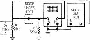
You can use an oscilloscope to graphically display the forward- and back-resistance characteristics of a diode. a test circuit used in conjunction with an oscilloscope is shown in figure 2-7. This circuit uses an audio-signal generator as the test signal. It should be adjusted for an approximate 2-volt, 60-hertz signal, as measured across R1.
Figure 2-7. - Display circuit used with an oscilloscope.
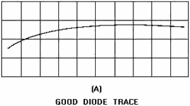
The test signal you apply to the diode is also connected to the horizontal input of the oscilloscope. The horizontal sweep will then display the voltage applied to the diode under test. The voltage developed across current-measuring resistor R2 is applied to the vertical input of the oscilloscope. Since this voltage is proportional to the current through the diode under test, the vertical deflection will indicate diode current. The resulting oscilloscope trace will be similar to the curve shown in figure 2-8.
2-17
Figure 2-8. - Typical characteristic curve of a silicone diode.
Reverse Voltage-Current Analysis
You can make an analysis of the reverse voltage-current portion of the characteristic curve for a diode with the method described above or with a diode test set. This test is very important for diodes used in computer applications, where stability of operation is essential. Various diode conditions that may be detected by this test are shown in figure 2-9, view A, view B, view C, and view D.
Figure 2-9A. - Diode reverse current-voltage characteristics. GOOD DIODE TRACE.
2-18
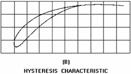
Figure 2-9B. - Diode reverse current-voltage characteristics. HYSTERESIs Characteristic.
Figure 2-9C. - Diode reverse current-voltage characteristics. FLUTTER (OR DRIFT) Characteristic.
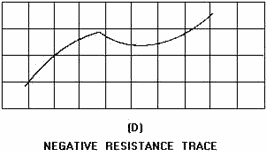
Figure 2-9D. - Diode reverse current-voltage characteristics. Negative Resistance TRACE.
2-19 Zener Diode Test
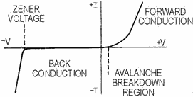
An audio signal generator may not be able to produce a high enough voltage for you to test Zener diodes. You can, however, make this test with a diode test set or with the circuit shown in figure 2-10. In this circuit, R1 is used to adjust the input voltage to a suitable value for the Zener diode being tested. Resistor R2 limits the current through the diode. The signal voltage applied to the diode is also connected to the horizontal input of the oscilloscope. The voltage developed across current-measuring resistor R3 is applied to the vertical input of the oscilloscope. The horizontal sweep will therefore represent the applied voltage, and the vertical deflection will indicate the current through the diode under test. Figure 2-11 shows the characteristic pattern of a Zener diode (note the sharp increase in current at the avalanche breakdown point). For the Zener diode to be acceptable, this voltage must be within the limits specified by the manufacturer.
Figure 2-10. - Zener diode test circuit.
Figure 2-11. - Zener diode characteristic pattern.
STATIC Resistance MEASUREMENTS One convenient method of testing a diode requires only your ohmmeter. The forward and back resistances can be measured at a voltage determined by the battery potential of the ohmmeter and the resistance range at which the meter is set. When the test leads of the ohmmeter are connected to the diode, a resistance will be measured that is different from the resistance indicated if the leads are reversed. The smaller value is called the forward resistance, and the larger value is called the back resistance. If the ratio of back-to-forward resistance is greater than 10 to 1, the diode should be capable of functioning as a rectifier. This is a very limited test, which does not take into account the action of the diode at voltages of
2-20
|
||||||||||||||||||||||||||||||||||||||||||||||||||